When Does a PCB Design Need Any-Layer HDI Instead of Conventional HDI?
A PCB design needs any-layer HDI when conventional HDI cannot provide the required layer connections within the available board space and thickness. This can happen with dense BGA packages, limited routing channels, and complex connections between internal layers.
However, not every high-density PCB needs any-layer interconnects. Conventional HDI may meet the same requirements with a simpler stackup and fewer manufacturing operations.
The decision should start with the actual routing requirements. Engineers need to review BGA escape routing, via connections, available layers, and manufacturing limits before selecting the structure.
What Makes Any-Layer HDI Different from Conventional HDI?
Both conventional HDI and any-layer HDI use microvias to increase routing density. The main difference is how these microvias connect the copper layers.
Conventional HDI Uses a Defined Buildup Structure
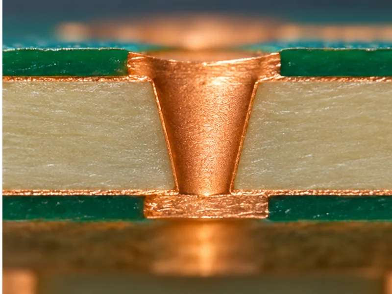
Conventional HDI boards commonly use a central core with additional buildup layers. Blind microvias connect selected outer layers, while buried vias or plated through-holes can provide other connections.
Common structures include 1+N+1 and 2+N+2. The numbers show how many buildup layers are added to each side of the central core.
For example, a 2+4+2 structure has eight copper layers. It contains four core layers and two buildup layers on each side.
This arrangement provides routing options without requiring microvias throughout the entire stackup. It works when the available connections can reach the required signal layers.
Engineers should select the buildup structure based on the actual routing paths. Adding more HDI stages does not automatically improve the design.
Any-Layer HDI Uses Microvias Throughout the Stackup
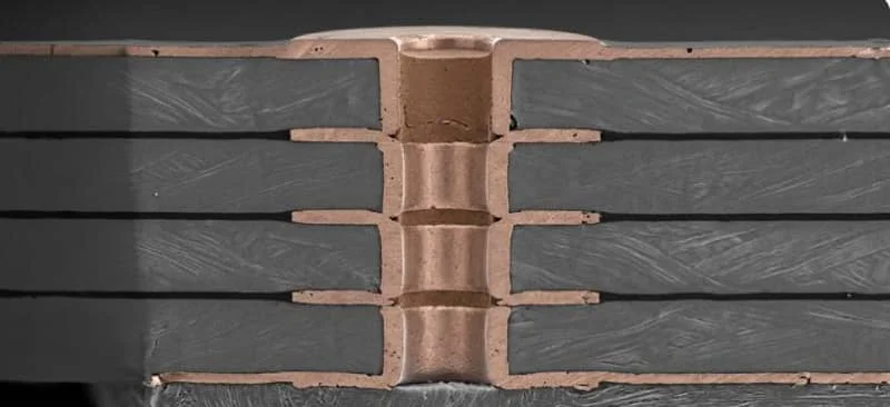
Any-layer HDI is also known as Every Layer Interconnect, or ELIC. It uses microvia connections between adjacent copper layers throughout the stackup.
A chain of microvias can connect signals across several layers. This gives designers more options for routing between layers.
However, any-layer does not mean that one laser-drilled microvia can directly connect any two layers across the board thickness. Each microvia has its own geometry, dielectric thickness, and manufacturing requirements.
The connections may use stacked copper-filled microvias. Their design must account for lamination, copper filling, registration, and reliability.
The main benefit is greater flexibility in selecting layer transitions. This becomes useful when conventional buildup connections cannot support the required routing.
When Does a PCB Design Need Any-Layer HDI?
Any-layer HDI becomes worth considering when routing problems remain after reasonable changes to component placement, layer assignments, and conventional via structures.
Engineers should identify the exact routing limitation before selecting ELIC.
Dense BGA Packages Need Access to More Routing Layers
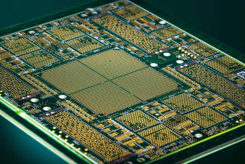
High-I/O BGA packages can create difficult breakout routing conditions. Inner rows of BGA pads may require additional routing layers to reach their connections.
Microvias help signals move away from these pads without using larger mechanically drilled vias. Via-in-pad structures can also preserve routing space around the package.
Consider a BGA package with a 0.5 mm pitch. The available space between pads may restrict conventional dog-bone fanout routing.
This is only a design example. A 0.5 mm BGA pitch does not automatically require ELIC.
The actual decision depends on the pad arrangement, pin count, signal assignments, trace width, spacing, and available routing layers.
A 1+N+1 or 2+N+2 HDI structure may provide enough connections. Any-layer HDI becomes more relevant when the required routing must reach layers beyond those available through the practical conventional buildup structure.
Limited Board Area Creates Routing Congestion
Compact products often place many components within a restricted PCB area. Connectors, mounting holes, power circuits, and mechanical keep-out zones can reduce the space available for routing.
Plated through-holes occupy space on layers they pass through. This can block routing channels even when a signal does not need connections on those layers.
Conventional HDI reduces this problem through blind and buried vias. These structures can free routing space compared with an equivalent layout using more through-holes.
However, a conventional core structure can still limit where some connections are placed. ELIC gives designers more options for reaching other layers through microvia connections.
The decision should be based on actual routing congestion. A smaller via footprint does not guarantee that the finished PCB will need fewer layers.
Board Thickness Restricts the Stackup
Some products have strict board thickness limits. The available space may be controlled by connectors, the enclosure, or mechanical assembly requirements.
A conventional HDI design may need additional buildup layers to complete the routing. Those layers can affect the total board thickness and dielectric arrangement.
Any-layer HDI allows engineers to consider different layer connection paths within a thin-layer stackup. This may help meet routing requirements when thickness is restricted.
However, ELIC does not guarantee a thinner PCB. Copper thickness, dielectric materials, impedance requirements, and mechanical strength still determine the final construction.
Both candidate stackups must meet the same electrical and mechanical requirements before thickness is compared.
How Can Engineers Decide Whether ELIC Is Necessary?
A useful comparison starts with the layer connections required by the design. Engineers should not select ELIC simply because a PCB has a high layer count or dense components.
The key question is whether conventional HDI can complete the routing without unacceptable electrical or mechanical compromises.
Check the Required Via Connections Between Layers
A via-span matrix helps engineers record the layer transitions needed by critical signals. It also shows where a conventional HDI structure may restrict routing.
For each critical connection, identify the starting layer, destination layer, and proposed via path. Then compare that path with the available buildup layers and manufacturing rules.
The following example assumes an eight-layer PCB. It is an illustrative design comparison, not a confirmed manufacturing stackup.
Required connection
Conventional HDI review
Any-layer HDI review
L1 to L2
Check surface microvia
Check adjacent-layer microvia
L1 to L3
Check available buildup connections
Review the required microvia sequence
L2 to L5
Review buried vias or combined transitions
Review available microvia paths
L1 to L8
Review through-hole or combined via options
Review the complete connection path
These connections describe routing requirements, not mandatory via structures. The actual implementation depends on the selected stackup and manufacturing capability.
If conventional HDI supports every required connection, ELIC may not be necessary. If routing still fails after reviewing placement, layer assignments, and via options, engineers can evaluate an any-layer structure.
The review must also consider signal integrity and reliability. More connection options do not automatically make a stackup better.
Check BGA Escape Routing Before Changing the Stackup
BGA escape routing should be reviewed early in the design. Engineers need to identify how many signal layers are required to route connections from the package.
A useful approach is to begin with the most congested BGA area. The layout team can test whether conventional microvias and available buried vias provide enough access.
If routing cannot be completed, the team should examine the remaining blocked connections. These results can show whether a different via structure is necessary.
ELIC should solve a specific routing limitation. It should not be selected before simpler HDI options have been evaluated.
Review Signal Integrity and Reference Planes
High-density routing also depends on the available reference planes. High-speed signals need suitable return paths and controlled impedance.
Microvias allow signals to change layers, but those transitions can introduce electrical discontinuities. The effects depend on via geometry, reference-plane arrangement, and signal frequency.
A design may have enough routing channels but still contain poor return paths. Adding more microvia connections does not solve that problem automatically.
Engineers should review layer transitions, reference-plane continuity, impedance, and power distribution together.
The selected structure must satisfy both routing density and electrical performance requirements.
What Manufacturing Challenges Come with Any-Layer HDI?
ELIC offers additional routing flexibility, but its construction requires careful control across multiple layers.
The manufacturing review must cover microvia geometry, copper filling, layer registration, and the required lamination sequence.
Sequential Lamination and Copper-Filled Microvias
HDI manufacturing may use several buildup operations. These processes can include dielectric preparation, laser drilling, copper deposition, plating, and lamination.
ELIC extends microvia connections throughout the stackup. Many structures require copper-filled microvias to support additional connections above them.
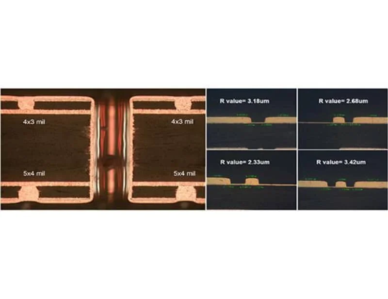
The manufacturer must control the copper filling and the interface between the microvia and its target pad. Weak interfaces or incomplete filling can affect the connection.
Layer registration is also important. A microvia must align with the required capture pad after the relevant manufacturing operations.
The proposed design should be reviewed against the manufacturer’s actual production rules. General HDI capability does not establish that every ELIC structure is manufacturable.
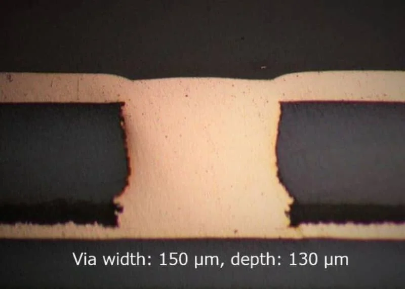
Microvia dimensions must match the selected dielectric structure. Hole diameter and depth affect drilling and plating requirements.
For example, a microvia with a 75 µm depth and a 100 µm diameter has an aspect ratio of 0.75:1.
This is a geometry calculation, not a universal production limit. The acceptable ratio depends on the material system, drilling process, plating method, and reliability requirements.
Microvia pad sizes and registration allowances must also be considered. Reducing the hole diameter does not automatically improve reliability.
Engineers should confirm these dimensions before the layout is released. Unverified microvia rules can lead to redesign or manufacturing problems.
Stacked Microvias Need Reliability Verification
Stacked microvias can connect several adjacent copper layers within a small area. They provide routing benefits, but the copper interfaces require careful manufacturing control.
Thermal loading during assembly can expose weak connections. Some defects may not become visible during initial bare-board inspection.
IPC has reported microvia interface failures that appeared after fabrication and conventional acceptance testing. These cases show why some complex structures need additional reliability evidence.
This does not mean all stacked microvias are unreliable. The risk depends on the actual structure, materials, manufacturing process, and thermal conditions.
Engineers should review the stacked via arrangement, number of connected levels, and product reliability requirements. They should also agree on suitable testing and acceptance criteria with the manufacturer.
The test plan must match the project. No single inspection method proves the reliability of every ELIC design.
How Does Any-Layer HDI Affect Manufacturing Cost?
Any-layer HDI can increase manufacturing complexity. However, its cost cannot be compared with conventional HDI using one fixed percentage.
The price difference depends on the actual stackup, via structure, materials, board dimensions, and manufacturing requirements.
Manufacturing Operations Affect Cost
Conventional HDI may use a limited number of buildup stages. This can reduce the manufacturing operations required for a design with moderate routing density.
An ELIC structure may need more extensive microvia drilling, copper filling, registration control, and lamination operations.
These processes affect manufacturing cost and may introduce additional production risks. Their impact depends on the exact design.
A lower layer count does not always mean lower manufacturing costs. A PCB with fewer layers but complex microvia connections may cost more to manufacture than a design using additional conventional layers.
Compare Stackups Under the Same Requirements
A meaningful cost comparison starts with two designs that meet the same product requirements.
Engineers should keep the electrical function, board dimensions, assembly requirements, and reliability targets consistent. Any changes between the options must be included in the comparison.
The manufacturing review should consider:
Copper layer count and dielectric construction
Material type and finished board thickness
Microvia quantity, geometry, and placement
Number and complexity of buildup operations
Copper filling and registration requirements
Inspection and reliability testing
Production quantity and panel utilization
These factors can affect the quotation in different ways. Their impact should be based on the actual manufacturing review rather than a general cost estimate.
If conventional HDI meets the design requirements, it may avoid unnecessary manufacturing complexity. ELIC becomes more valuable when its routing flexibility solves a problem that the simpler structure cannot resolve.
What Should Engineers Confirm Before Selecting ELIC?
The final decision should be based on a manufacturable stackup and verified routing requirements.
An engineer does not need to select ELIC at the beginning of every dense PCB project. The better approach is to identify the connections that conventional HDI cannot support.
Prepare the Stackup and Routing Requirements
The initial review should include the main components, routing constraints, and proposed layer connections.
The most useful information includes:
BGA package pitch, pin count, and pad arrangement
Required routing layers and via transitions
Proposed blind, buried, and stacked microvia structures
Minimum trace width and spacing
Finished board thickness and material requirements
Dielectric thickness and proposed microvia geometry
Controlled impedance and reference-plane requirements
Assembly temperature exposure and reliability requirements
This information helps engineers compare conventional HDI and ELIC using the same design targets.
If the requirements can be met with conventional HDI, a more complex structure may offer no practical advantage.
Verify Manufacturing Capability for the Exact Structure
ELIC manufacturing capability must be evaluated against the proposed stackup. A supplier’s general HDI service description is not enough to confirm every possible layer connection.
Before choosing an ELIC stackup, engineers should confirm the proposed microvia structure, materials, layer connections, and reliability requirements with the PCB manufacturer.
The review should also cover copper filling, registration, lamination operations, and available inspection methods.
Our HDI PCB manufacturing page provides information about HDI fabrication and engineering review. A specific any-layer construction still requires confirmation against the project’s technical requirements.
Choose the Simplest Stackup That Meets the Requirements
Any-layer HDI is worth considering when conventional HDI cannot provide the routing access needed by the design. Dense BGA areas, restricted routing space, and complex internal connections can create these conditions.
Conventional HDI remains suitable when its buildup layers and available via structures can complete the routing.
Engineers should compare both options using routing results, electrical requirements, board thickness, manufacturing feasibility, cost, and reliability evidence.
Choose the simplest stackup that meets these requirements. ELIC should be a response to a demonstrated design need, not a default choice for every high-density PCB.
Before releasing an any-layer stackup, agree with the fabricator which microvia fill and registration checks apply to the proposed structure. A cross-section or fill review on the actual build-up is more useful than a generic HDI capability claim.
Need a manufacturability check? Compare our HDI PCB overview and sequential lamination and stacked vias notes, then send BGA pitch, the proposed stackup, and any thickness limits via Contact Us. Topline Circuit will review whether conventional HDI can still meet the routing before an ELIC construction is quoted.
Engineering Support for Your PCB Project
Need help with your PCB or assembly project? Contact our team to discuss your design, manufacturing and testing requirements.
Inconsistent solder paste deposits on fine-pitch HDI pads can result from poor paste release from the stencil, uneven board support, problems with paste storage or handling, or incorrect printer settings. The HDI
PCB board technology is how modern electronics get both mechanical support and copper interconnects on a single laminate—pads, traces, vias, layers, and materials that determine density, speed, heat, and cost. By the
The cost of a 10-layer rigid PCB depends on its size, materials, copper weight, hole structure, and manufacturing requirements. Order quantity, testing, and delivery timing also affect the quote. Two boards with
To provide the best experiences, we use technologies like cookies to store and/or access device information. Consenting to these technologies will allow us to process data such as browsing behavior or unique IDs on this site. Not consenting or withdrawing consent, may adversely affect certain features and functions.
Functional
Always active
The technical storage or access is strictly necessary for the legitimate purpose of enabling the use of a specific service explicitly requested by the subscriber or user, or for the sole purpose of carrying out the transmission of a communication over an electronic communications network.
Preferences
The technical storage or access is necessary for the legitimate purpose of storing preferences that are not requested by the subscriber or user.
Statistics
The technical storage or access that is used exclusively for statistical purposes.The technical storage or access that is used exclusively for anonymous statistical purposes. Without a subpoena, voluntary compliance on the part of your Internet Service Provider, or additional records from a third party, information stored or retrieved for this purpose alone cannot usually be used to identify you.
Marketing
The technical storage or access is required to create user profiles to send advertising, or to track the user on a website or across several websites for similar marketing purposes.
 Skip to content