 Skip to content


Check Copper Patterns During PCB Fabrication
Topline Circuit uses automated optical inspection to check manufactured copper patterns against the approved production reference. Bare-board AOI supports the review of visible conductor defects on inner and outer layers during fabrication.
Send your board files, critical conductor requirements and inspection-record needs. We review the layer scope, acceptance criteria and complementary electrical tests with your manufacturing order.
Compare the Copper Pattern with the Released Data
AOI scans the accessible copper pattern and compares its features with a reference prepared from the approved manufacturing data. The inspection program identifies differences that require review.
Reference alignment, layer identity and program revision matter. A finding is evaluated against the drawing and applicable acceptance criteria before it is classified as a confirmed defect.

Copper Features Reviewed by AOI
| Feature | Optical review focus |
|---|---|
| Conductor gaps | Visible breaks or missing copper in a trace or connection. |
| Copper bridges | Unwanted copper connecting features that should remain separate. |
| Local width and spacing | Narrowed conductors or reduced gaps relative to the programmed criteria. |
| Excess or missing copper | Residual copper, protrusions, notches and other visible pattern deviations. |
| Pad and plane features | Visible geometry differences in lands, clearances and plane openings. |
Inspect Inner Layers Before Lamination
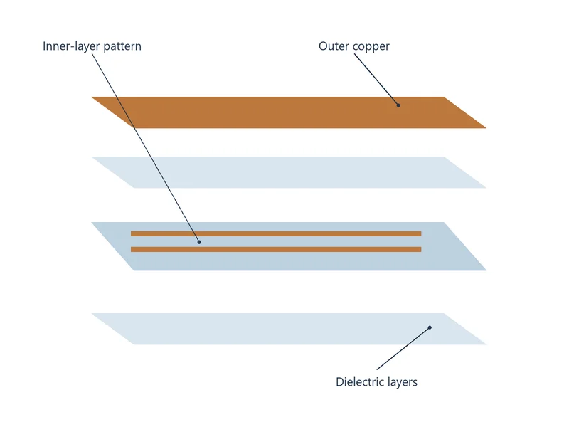
Inner-layer copper is inspected while it is still optically accessible, before the multilayer stack is laminated. Suspect locations can then be reviewed before they become enclosed in the board.
Outer-layer AOI checks the accessible conductor pattern after the relevant pattern-forming stages. Define the layers and inspection stages with the board construction rather than treating one final surface scan as inspection of every layer.
Define the Inspection Scope and Acceptance
- Released reference: identify the board revision, layer sequence and approved manufacturing data.
- Layer coverage: specify the inner or outer layers and process stages requiring inspection.
- Critical geometry: provide conductor width, spacing and pad requirements with tolerances where specified.
- Acceptance basis: identify the applicable specification, revision, class and any customer-specific criteria.
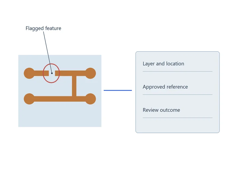
- Review records: request layer and location identification, images, confirmed findings and follow-up results as required.
Review Findings Before the Next Process Step
A machine call can represent a real pattern defect or an acceptable condition that needs confirmation. Review the image, physical feature and approved reference together before deciding the next action.
Boards or panels with confirmed defects are held while the next action is agreed. Where correction is permitted and authorized, the affected features are checked again before the items move to the next applicable process stage.
Combine AOI with Bare-Board Electrical Testing
AOI evaluates visible copper geometry. Electrical testing checks continuity and isolation against the approved electrical reference; it can address connections that are not accessible to an optical view.
Optical inspection does not establish hole-wall plating thickness, complete internal construction or functional operation of an assembled product. Include the required electrical and construction checks in the inspection plan. See our PCB testing and inspection services for the broader scope.
Files for a Bare PCB AOI Review
- Gerber or ODB++ copper-layer data with clear layer names
- Fabrication drawing, stack-up and board revision
- Critical conductor dimensions and agreed acceptance requirements
- Requested layer coverage, inspection stages and records
- A design netlist, if available, electrical-test requirements and order quantity
AOI is coordinated with our PCB fabrication services. Identify any first-article review or approval hold point before the order is released.
Bare PCB AOI FAQs
No. AOI checks accessible copper geometry, while electrical testing checks continuity and isolation using the approved electrical reference. Specify both where required, especially for multilayer connections that cannot be inspected optically after lamination.
Ordinary optical inspection cannot see copper through an opaque laminated stack. Specify inner-layer AOI before lamination. If a completed board is suspected of an internal defect, provide the affected nets and failure evidence so suitable electrical or construction-analysis methods can be reviewed.
Check the flagged location against the physical feature, approved reference and acceptance criteria. If a defect is confirmed, hold the affected board or panel and review permitted correction, replacement or a formally approved deviation. Reinspect corrected features and perform the applicable electrical tests before release.
Not by itself. A trace may conduct while still falling outside the specified geometry. Compare the measured feature with the drawing and acceptance criteria, then assess any deviation through the approved review process rather than using continuity alone as acceptance.
Send the complete released layer set, drawing, stack-up and revision identifier. Identify changed features and remove obsolete files from the production package. Confirm that the optical reference and any electrical-test data correspond to the same approved revision.
Specify the layers, locations or record types needed during quotation review. Include the board or lot identifier, required image format and any review hold points. We confirm the available records and scope before production; a summary pass result is different from a location-specific finding and its review outcome.
Discuss Your Bare-Board Inspection Requirements
Send your board files, layer scope and required records. We will review the optical inspection and electrical-test requirements with your PCB manufacturing order.