 Skip to content


SMT Stencils Matched to Your Board and Printing Setup
We provide laser-cut stainless steel PCB stencils for solder paste printing, with framed, frameless and stepped options. We review your paste layers, panel layout and printing requirements to define the foil, apertures and mounting arrangement.
Send the final board or panel files and identify the components with critical paste-volume requirements. You can specify a thickness or request an engineering review before approving the stencil design.
Choose the Mounting Arrangement for Your Printer
A framed stencil holds the foil in a dedicated support assembly. A frameless foil needs a compatible reusable tensioning system or a suitable manual printing fixture.
Specify the printer or holder, outer dimensions, mounting interface and required print area. Confirm the usable aperture area separately from the frame size so the complete panel fits within the supported printing zone.

PCB Stencil Options and Specifications
| Item | Available options | Ordering details |
|---|---|---|
| Material and cutting | Laser-cut stainless steel | Provide approved paste layers and the final board or panel outline |
| Mounting | Framed or frameless | Specify frame dimensions or the compatible holder and tensioning interface |
| Foil thickness | 0.08, 0.10, 0.12, 0.15, 0.20, 0.25 and 0.30 mm | Select using the actual aperture geometry, solder paste and required deposits; 0.10 mm = 100 µm |
| Foil profile | Single thickness or stepped construction | Define local thickness zones and the available clearance around each transition |
| Printing sides | Top, bottom or both | Confirm whether both patterns share one foil or use separate stencils |
| Surface treatment | Electropolishing and nano-coating options | Identify the paste-release or cleaning requirement being addressed |
| Fiducials | Half-etched or through-cut patterns, or none where appropriate | Match the printer vision system and approved panel coordinates |
| Dimensions and layout | Printer-compatible frame or custom foil layout | Specify outer dimensions, usable print area, orientation and number of boards per panel |
Review Thickness and Apertures Together
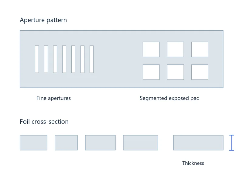
Foil thickness and aperture geometry jointly influence the amount of paste available for printing. Review fine-pitch leads, small components, exposed pads and larger connector lands together rather than selecting thickness from package names alone.
Confirm paste requirements and any component-specific land-pattern guidance. Where one thickness cannot meet the different deposit requirements, evaluate aperture changes and local step thicknesses before approving the production file.
Use Step Stencils for Defined Deposit Requirements
A stepped stencil uses different local foil thicknesses to address deposit requirements within the same print. Mark each zone, its thickness and transition position on the approved drawing.
Review nearby apertures, squeegee travel and printer clearance around the steps. Electropolishing and coatings are separate process choices; they do not replace the need for suitable aperture geometry and printing conditions.
Match the Stencil to the Released Panel
Use the final panel layout, including board spacing, orientation, rails and fiducials. Identify the top and bottom paste layers, coordinate origin and viewing convention so the approved output matches the intended printing side. Confirm any required mirroring in the approved drawing rather than mirroring the files independently.
Mark DNP positions and pads that must receive no paste. If top and bottom patterns share one foil, review their separation, support and clamping arrangement before cutting.

Check the Finished Stencil and Validate the Print
Review aperture position and geometry, foil thickness, blocked openings, edge condition and identification against the approved specification. Check frame or holder compatibility and the print area before setting up the job.
Use a trial print to verify alignment and deposits with the actual paste, board support and printer settings. For SMT PCB assembly, define the required solder paste inspection and acceptance criteria before placement.
Files for a PCB Stencil Quote
- Top and/or bottom paste Gerber files with revision and layer identification
- Final PCB or panel outline, spacing, rails and fiducial coordinates
- Framed or frameless construction and printer or holder requirements
- Outer dimensions and required usable printing area, in millimetres
- Selected foil thickness, or a request for thickness and aperture review
- Critical component drawings and paste recommendations where available
- DNP positions, aperture changes and any stepped thickness zones
- Quantity, surface treatment, identification and packaging requirements
State whether you need a separate stencil shipment or tooling for a PCB assembly order. If files are preliminary, identify the open items so the cutting file can be approved before manufacture.
PCB Stencil FAQs
Yes. Send the paste layers, final panel layout and details of critical components, together with the intended paste and printing method where available. Identify the smallest apertures and any large exposed pads so the review covers both paste release and deposit volume. Approve the selected thickness and cutting file before manufacture.
They can share a foil when the usable area and printing fixture accommodate both patterns. Provide both paste layers and confirm how each pattern will be aligned, supported and clamped. Separate stencils may be more practical when the patterns or production setup require independent mounting.
Compare the new panel with the approved stencil file before reuse. Check board spacing, orientation, pad coordinates, fiducials and clamping positions, as well as any component or DNP changes. A matching single-board design does not ensure that a changed panel will align with the existing stencil.
Send the PCB data, assembly drawing, BOM and relevant component guidance. Identify DNP positions, exposed pads and any parts to be soldered later. We can review the information needed to prepare apertures, but the copper pads should not be copied directly without considering paste requirements. Approve the resulting paste pattern before cutting.
Identify the competing deposit requirements using the actual component and pad geometry. Review aperture sizes and segmentation of large exposed-pad openings together with the foil thickness. If a single thickness is unsuitable, evaluate stepped zones or another defined deposition process, then validate the selected design with a trial print.
Stop placement on affected boards and inspect alignment, board support, stencil cleanliness and contact with the board. Check paste condition and the supplier-recommended printing and separation settings. Compare aperture geometry and thickness with the approved file before deciding whether a stencil change is needed. Clean or reprint affected boards using the approved process, then recheck deposits before placing components.
Discuss Your Stencil and Printing Requirements
Send your paste layers, final panel layout and printer details. We will review the stencil construction, thickness and aperture requirements for your order.