 Skip to content


Remove Unused Via Stubs from High-Speed Connections
Topline Circuit provides PCB backdrilling for multilayer boards, backplanes and high-speed interconnections. We support top-side, bottom-side and multi-depth backdrill plans for prototype and production orders.
Send your stack-up, via locations and residual-stub requirements. We review drill access, protected connections and copper clearances before preparing the manufacturing plan.
Keep the Connection, Remove the Unused Barrel
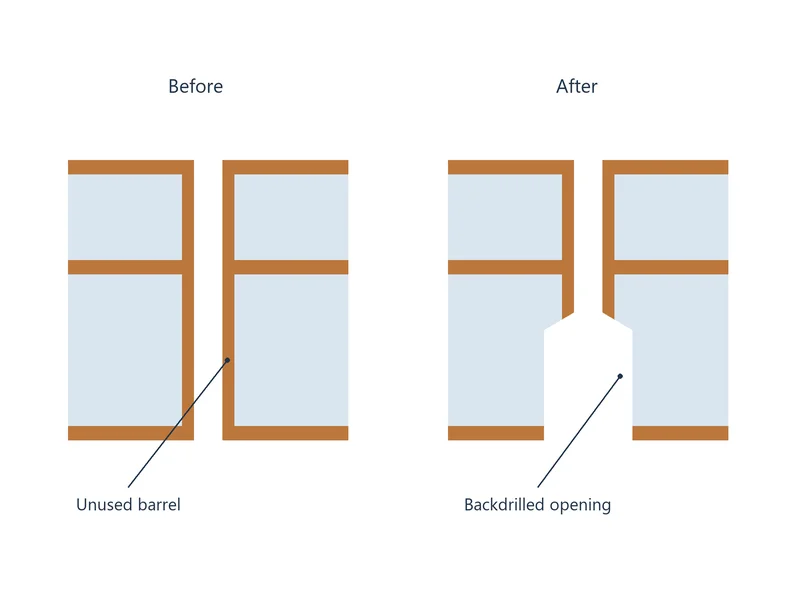
A plated through-via can extend beyond the layers used by a signal. This unused copper barrel forms a stub that can affect the via transition.
Backdrilling removes the unwanted barrel with a larger drill at a controlled depth. The process leaves the required connections intact and a specified residual stub near the last functional connection.
Choose the Vias That Need Backdrilling
Use channel analysis, connector guidance and the actual via structure to identify the connections that need stub removal. Review signal bandwidth, rise time, material properties and the length of the unused barrel together.
An impedance-controlled board does not automatically require backdrilling. Select the relevant via groups and compare the routing, stack-up and manufacturing cost with blind-via or microvia alternatives.
Define the Entry Side and Protected Layer

For each backdrill group, identify whether the drill enters from the top or bottom. State the last functional connection and the layer that must not be cut.
Separate groups that use different directions, diameters or depths. For double-sided backdrilling, identify the retained barrel and all required layer connections so neither operation removes a functional interconnect.
Backdrill Requirements for Manufacturing
| Requirement | What to define |
|---|---|
| Entry side and layer span | Top or bottom entry, affected via group and protected functional layers. |
| Residual stub | Maximum allowed remaining copper stub and the measurement basis relative to the functional connection. |
| Protected connection | The minimum separation or other specified acceptance criterion that prevents damage to the functional pad and barrel. |
| Drill diameter | Original production drill diameter, backdrill diameter and registration requirements. Do not substitute the plated finished opening for the original tool size. |
| Copper clearance | Edge-to-edge clearance from the backdrill envelope to nearby copper that must be retained. Include tool diameter and drill-location tolerance in the clearance review. |
| Stack-up and depth control | Layer depths, board thickness and tolerances, with the process depth agreed against the residual-stub and protected-layer requirements. |
Residual Stub and Drill Depth Are Different
Drill depth is measured from the entry surface to the specified tool reference, such as the drill tip. Residual stub describes the unused conductive barrel left near the functional connection after drilling.
Layer position, laminated thickness, depth variation and drill-tip geometry affect the result. We review these together rather than treating a machine depth tolerance as the residual-stub tolerance.

Manufacture and Verify the Backdrilled Features
We review the drill data with the approved stack-up, align the backdrill operation to the plated holes and machine the selected groups. The holes are cleaned and checked for remaining debris and visible defects.
Agreed microsections and representative coupons assess the residual stub and retained connections. Electrical testing checks continuity and isolation; it does not replace dimensional inspection or demonstrate the performance of the completed signal channel.
Files for a Backdrilled PCB Quote
- Gerber or ODB++ data, primary drill files and a fabrication drawing
- Separate backdrill files or a clearly identified via map for each entry side and depth group
- Stack-up with layer names, materials, thicknesses and tolerances
- Protected functional layers and residual-stub requirements for each group
- Original drill and backdrill diameters, copper keep-outs and required inspection records
- Quantity and connector or channel requirements relevant to the backdrill plan
Our PCB DFM review checks the drill plan with the surrounding copper and stack-up. See our PCB fabrication services for the wider manufacturing scope.
PCB Backdrilling FAQs
Identify signal vias whose unused barrel affects the required channel performance. Use the connector recommendations or channel analysis to select them. Mark their locations and retained layer connections instead of applying one backdrill rule to every via on the board.
Do not use zero as an unconditional drilling target. Removing all copper up to the functional connection can damage the pad or barrel. Specify the maximum residual allowed by the electrical design and the protection requirement for the active connection, then review the achievable range with the stack-up.
Provide a separate group for each entry side and span. Identify the entry surface, last functional connection and must-not-cut layer in the drawing. Add the residual-stub requirement and measurement basis so CAM can translate the design intent into a drill depth.
Confirm that the measurement uses the agreed functional-layer reference and compare it with the specified maximum stub. Hold the affected boards if the limit is exceeded. Provide the backdrill group, location and microsection report for review. Additional drilling requires a check of the remaining margin to the protected connection; agree on rework or replacement before proceeding.
Treat this as a rework review, not an automatic drilling operation. Provide the original manufacturing files, actual stack-up, via locations, surface finish and assembly status. Check tooling access, retained connections, nearby parts, cleanliness and inspection before approving rework. Replacement may be needed if the structure or access does not support it.
Compare the required layer connection, available routing space and stack-up. Backdrilling removes an unused part of a plated through-via; blind vias stop at a selected layer during fabrication. Review the protected-layer margin, oversized-hole clearance and lamination requirements for each route before choosing.
Review Your Backdrill Plan
Send your board files, stack-up and via groups. We will review the retained connections, residual-stub requirements and manufacturing route before preparing a quotation.