 Skip to content


Size the Copper Around the Hole
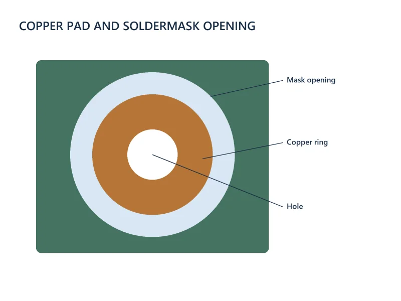
An annular ring is the copper surrounding a hole within a pad. We review the pad, hole and registration requirements together to help you prepare a manufacturable PCB design.
Send your board files, hole requirements and any fixed layout constraints. We check the available copper margin and discuss changes with your team before production.
Calculate the Nominal Ring Width
For a round hole centered in a circular pad:
Nominal radial ring width = (pad diameter – stated hole diameter) / 2
A 0.60 mm pad with a centered 0.30 mm hole gives a nominal ring width of 0.15 mm. This is a geometry example, not a minimum manufacturing specification.
State what the hole diameter represents. A calculation using the finished hole opening does not describe the same geometry as one using the larger production drill.
Production Drill and Finished Hole
Plating reduces the opening of a mechanically drilled plated hole. The production drill is selected to achieve the specified finished hole within its tolerance.
We review the pad against the applicable production drill and registration requirements. Drill compensation depends on the construction and process; do not apply one fixed allowance to every hole.
Offset Holes and Other Pad Shapes
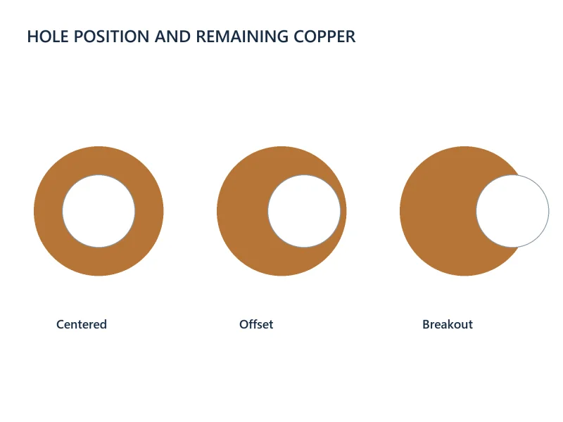
A centered-hole calculation does not show the minimum copper width after misregistration. An offset hole leaves less copper on one side and more on the other.
For oval pads, slots or other shapes, evaluate the local copper distance around the actual feature. Do not treat the circular-pad formula as a complete acceptance check.

Separate Design Rules from Acceptance Criteria
Nominal Design Geometry
Your CAD rule checks the geometry defined in the design. Confirm that its hole definition and layer rules match the manufacturing requirements.
Manufacturing Margin
Drill position, layer registration, hole size and etched pad dimensions affect the remaining copper. Review these factors together before using a supplier’s smallest advertised feature as the default design rule.
Finished-Board Acceptance
Specify the applicable acceptance document, revision and product class. Ring and breakout requirements must be matched to the layer and hole type being inspected.
Review Inner and Outer Layers Separately
A centered outer-layer hole does not prove that every internal land is aligned. We review internal pads, registration requirements and clearances as part of the complete stack-up.
Through holes, blind vias and microvias also need different process checks. Define capture pads, target pads and layer spans for the selected via structure.
Resolve Insufficient Annular Ring Width
Increase the Pad Where Space Allows
A larger pad can provide more copper margin. Check nearby traces, pads, copper clearances and soldermask requirements before approving the change.
Review the Hole Requirement
A smaller hole can increase the nominal ring width, but it must still meet the design requirements. For component holes, check lead dimensions, insertion clearance, finished-hole tolerance and assembly requirements.
For vias, review plating, aspect ratio, electrical requirements and the production process. Do not reduce a specified finished hole solely to clear a DFM warning.
Rework the Routing or Via Structure
Where the pad cannot grow, compare another via position, routing arrangement or suitable interconnect structure. Review the manufacturing cost and constraints before updating the files.
Use Teardrops for the Right Purpose
A teardrop adds copper locally where a trace joins a pad. It does not increase the copper margin around the entire hole or replace the specified ring and clearance requirements.
Keep Copper and Soldermask Requirements Separate
Soldermask expansion controls the opening around a pad. Enlarging that opening does not add copper to the annular ring.
Review copper geometry and mask registration separately. Mark any changes that require customer approval before fabrication.
Files for an Annular Ring Review
Send the available design package and identify the affected features:
- Copper layers in Gerber or ODB++ format
- Drill files and the definition of each stated hole size
- Finished-hole sizes and tolerances where required
- Layer stack-up, materials and copper requirements
- Via spans, pad sizes and relevant clearances
- Component lead dimensions for affected insertion holes
- Applicable acceptance requirements and fixed layout constraints
Our PCB DFM review checks hole sizes, annular rings and drill-to-copper spacing together. Include the reviewed requirements with your PCB fabrication enquiry.
Annular Ring FAQs
The CAD check may use a nominal hole size or a rule that differs from the production process. Compare the CAD pad and hole definitions with the proposed drill, layer registration and acceptance requirements. Send the affected padstack and drill data so the difference can be identified before changing the layout.
State the purpose of the calculation first. A finished-opening calculation describes nominal surface geometry, while a manufacturing check must account for the applicable production drill and process tolerances. Send the required finished hole and pad size so we can confirm the manufacturing basis.
Only if the revised hole still meets the electrical, mechanical and assembly requirements. For a component hole, provide the lead dimensions and insertion requirements. For a via, provide the stack-up and required connection so the hole, plating and aspect ratio can be reviewed together.
They can add copper at the trace-to-pad junction, but they do not restore the required copper width around the entire hole. Check the actual deficiency first. A pad, hole, routing or process change may be needed in addition to a teardrop.
Not from appearance alone. Evaluate the remaining ring, trace connection and any breakout against the specified acceptance requirements for that layer and hole type. Provide the drawing requirements and inspection evidence so the feature can be assessed on the correct basis.
Send the affected area, padstack, drill data and fixed component constraints. We can compare permitted hole changes, local routing changes or another suitable via structure. Approve the revised geometry and manufacturing requirements before production.