 Skip to content


Bond the Approved Layers into a Multilayer PCB
We provide PCB lamination services as part of multilayer board fabrication. We bond the specified cores, bonding materials and copper foils into the approved construction, with the process selected for the material system and board requirements.
Send your layer stack-up, materials, copper thickness and quantity. Identify critical dielectric spacing, total board thickness and via structures so we can review the lay-up and pressing route before production.
Prepare the Materials and Inner Layers for Bonding
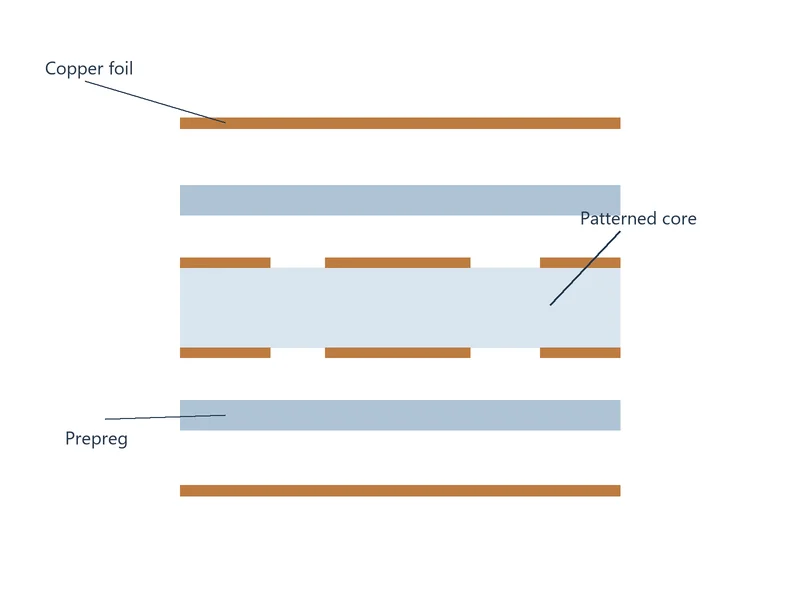
Cores provide cured dielectric layers and the required copper patterns. During pressing, prepreg resin flows around the copper features and cures to bond the layers. Other bonding materials are processed according to their specified requirements.
Before lay-up, we review the material identity, layer order and inner-layer inspection requirements. Surface preparation and material handling are selected for the bonding system and board construction.
Define the Finished Construction Before Pressing
| Requirement | What to specify | Manufacturing review |
|---|---|---|
| Layer order and materials | Core grades, bonding materials, copper layers and approved sequence. | Material compatibility, bonding interfaces and the required construction. |
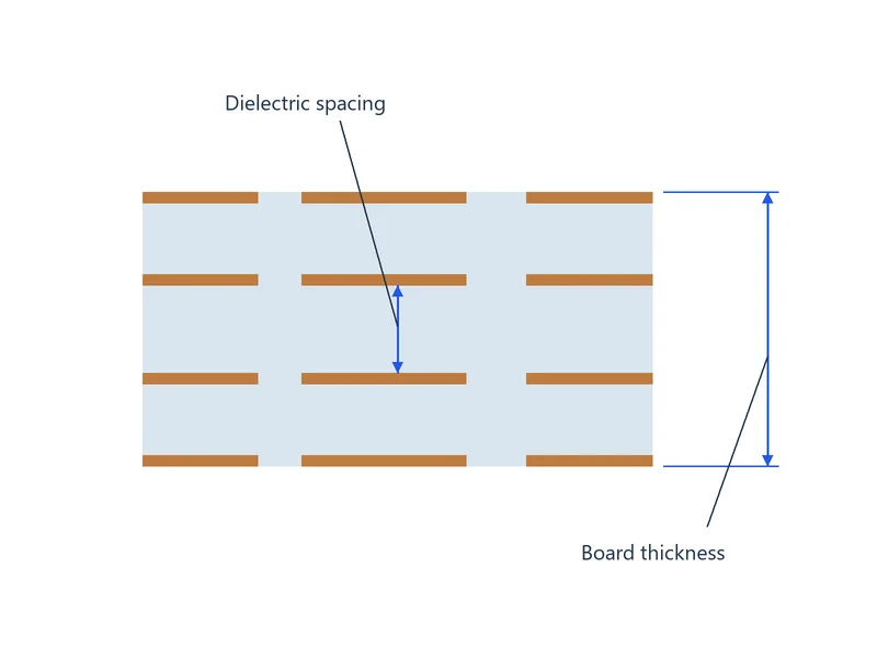
| Finished board thickness | Total thickness, tolerance and whether copper, solder mask or other coatings are included in the measurement. | Combined effects of the material stack, copper and pressing process. |
| Pressed dielectric spacing | Required spacing between identified copper layers, with tolerance and measurement locations where critical. | Core thickness, bonding-material construction, resin flow and copper distribution. |
| Copper requirements | Layer-by-layer copper thickness and any heavy-copper areas. | Resin filling around copper features and balance across the construction. |
| Via structure | Through, blind, buried or stacked connections with the layer spans identified. | Whether the design requires a single bonding stage or sequential construction. |
| Acceptance and records | Applicable drawing, specification, revision and required measurements or inspection records. | Inspection locations, sampling and any additional qualification requirements. |
Control Lay-Up, Registration and the Bonding Cycle
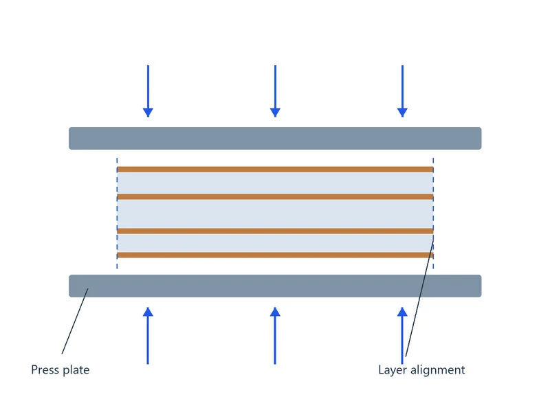
We align the prepared layers to the approved sequence and plan the pressing cycle for the specified materials. Heat, pressure, vacuum where used, and controlled cooling work together with the resin flow and cure requirements.
The required cycle is material-specific. Material Tg is not a press-temperature setting, and a vacuum-assisted process does not by itself prove that every bonded interface is free of voids.
Review Pressed Thickness with Electrical Requirements
Dry prepreg thickness is not the same as its thickness after bonding. Resin content, copper patterns and processing affect the resulting dielectric spacing and total board thickness.
For impedance-controlled layers, we review the pressed spacing together with conductor geometry and material properties. Proposed changes to the bonding material or stack-up are checked against the approved electrical and mechanical requirements before production.
Verify Thickness and Bonded-Layer Construction
Inspection can include finished thickness, layer registration and microsections at the agreed locations. We review the specified evidence for resin filling, bonded interfaces and layer construction, with additional tests where required.
When inspection identifies a confirmed nonconformance, we hold the affected material for disposition. Further analysis and any authorized correction must be followed by the required verification before release.
Match the Bonding Route to the Design
- Conventional multilayer construction: combines prepared layers in the approved lay-up and bonding sequence.
- Sequential lamination: builds and processes substructures in stages to create the specified interconnections.
- Hybrid construction: requires compatible cores and bonding materials, with the thermal and electrical requirements reviewed together.
- Heavy copper: requires suitable resin filling, dielectric spacing and copper distribution.
Our sequential lamination and stacked-via service covers staged build-up structures. See our HDI PCB manufacturing service for related microvia constructions.
Files for a PCB Lamination Review
- Approved layer stack-up and fabrication drawing
- Material grades, core construction and specified bonding materials
- Copper-layer files and layer-by-layer copper thickness
- Total board thickness, tolerance and measurement basis
- Critical dielectric spacing, impedance targets and permitted adjustments
- Via layer spans, assembly thermal requirements and requested inspection records
We coordinate bonding with our PCB fabrication services. Identify material substitutions or stack-up changes that require approval before manufacturing release.
PCB Lamination FAQs
Check whether the quoted values describe bare dielectric, copper-clad cores or dry bonding sheets. Bonding changes prepreg thickness as resin flows around the copper patterns. Provide the required finished thickness, tolerance and measurement basis so we can review the pressed construction rather than simply adding nominal sheet values.
Compatible hybrid constructions can be manufactured, but the exact core and bonding-material grades must be reviewed together. Send the layer order, material grades, copper requirements and electrical targets. We review bonding compatibility and the processing requirements before approving the construction or a proposed material change.
It can change the pressed dielectric spacing and electrical properties of the construction. Identify the affected layers and impedance requirements before making the substitution. We review the proposed material and geometry, obtain the required approval and define any impedance verification needed for the revised build.
Provide the stack-up and the start and stop layers of each via group. Buried connections and staged microvia structures may require processing substructures before additional layers are bonded. We plan the manufacturing sequence from those connections; layer count alone does not determine the number of bonding stages.
Set aside the affected boards and record the lot identity, locations, photographs and thermal or handling history. Compare measured warpage and other findings with the agreed criteria. We review suitable analysis and any further sampling, then agree on disposition and required verification before release; a surface photograph alone may not establish an internal defect.
Yes. Identify the layer pairs, thickness limits, measurement locations and required report format during quotation review. Agree whether the evidence is from the board or a representative coupon, together with the sampling plan. Include traceability and any specified conditioning so the results can be interpreted against the required construction.
Discuss Your PCB Bonding Requirements
Send your stack-up, material specifications and critical thickness requirements. We will review the lamination route, proposed construction and required inspection records with your PCB order.