 Skip to content


Solderable Pads with Integrated Vias
Topline Circuit manufactures via-in-pad PCBs for BGA, fine-pitch and other compact component layouts. We support filled and copper-capped vias, including VIPPO constructions, from prototypes to production.
Send your component land patterns, stack-up and via requirements. We review the via structure and finished pad surface together so the board can support the planned routing and assembly process.
Via-in-Pad and VIPPO
Via-in-pad describes the location of a via inside a component pad. Via-in-pad plated over, or VIPPO, describes a filled, planarized and copper-capped construction that provides a continuous copper surface over the via.
The fill supports the cap; the cap becomes part of the pad structure. Soldermask tenting or plugging does not create the same solderable copper surface.

Choose the Fan-Out Around the Package
| Layout | How it routes | What to review |
|---|---|---|
| Dog-bone fan-out | A short trace connects the component pad to a separate via. | Space for the via land, trace and clearances between adjacent pads. |
| Via-in-pad | The via sits within the component pad and connects to the required layer. | Via diameter, pad size, layer span, filling and the finished solderable surface. |
Match the Via Structure to the Stack-Up
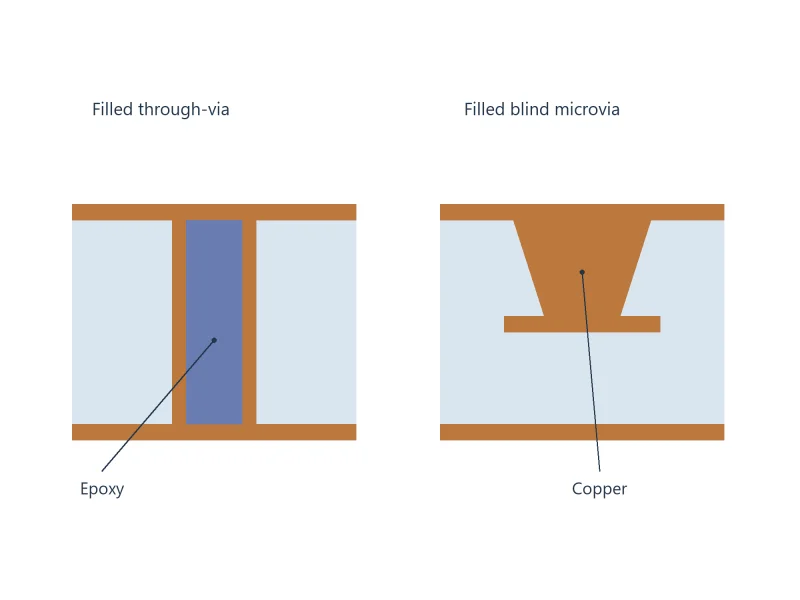
A resin-filled, copper-capped through-via can provide a via-in-pad connection in a conventional multilayer board. Copper-filled laser microvias provide shorter layer connections in suitable build-up structures.
Select the via layer span to suit the escape routing and stack-up. A via inside a pad does not automatically require stacked microvias or sequential lamination. Our filled via manufacturing services cover the filling options behind these constructions.
Define the Pad and Via Requirements
- Component land pattern: provide pad size, pitch, soldermask openings and the package drawing.
- Via geometry: identify the production drill diameter or laser opening, via depth, layer span and capture-pad dimensions. Distinguish the tool size from the plated opening before filling. For mechanically drilled vias, state the drilled depth and tool diameter used for the aspect ratio; review laser-microvia depth and opening geometry separately.
- Copper registration: review the remaining copper around the via with drill alignment and pad tolerances.
- Fill and cap: specify the filling material, capped sides and copper-cap thickness requirements.
- Surface condition: define acceptable dimples, protrusions and planarity for the intended assembly.
- Finished surface: identify the surface finish and any package-specific assembly requirements.
Review the Finished Pad with Assembly
An open via in a solder pad can draw solder away from the joint. Filled-and-capped construction closes that opening, while pad planarity supports consistent stencil contact and component seating.
Review the package land pattern, soldermask, stencil aperture and reflow process together. For exposed thermal pads, follow the device-specific via and solder-paste recommendations rather than applying one treatment to every package.

Manufacturing and Verification
For resin-filled VIPPO, we prepare and plate the via, fill and cure the resin, planarize the surface and form the specified copper cap. Copper-filled microvias use an electroplating route selected for their geometry and build-up sequence.
Surface inspection checks the finished pad condition. Electrical testing checks continuity and isolation; microsections and other agreed methods assess internal filling and cap construction. Assembly inspection evaluates the resulting solder joints against the assembly requirements.
Files for a Via-in-Pad PCB Quote
- Gerber or ODB++ data, drill files and a fabrication drawing
- Stack-up and a via map showing layer spans and the pads containing vias
- Component package drawings and land patterns
- Filling material, copper capping, planarity and surface-finish requirements
- Quantity and required inspection records
- BOM, placement data and an assembly drawing when assembly is included
Our PCB DFM review checks the pad and via data before manufacturing. Identify fixed layout constraints so proposed changes can be reviewed before the production files are approved.
Via-in-Pad PCB FAQs
A soldermask plug does not provide a solderable copper cap. Where the BGA pad needs a continuous surface, specify filling, planarization and copper capping, together with the pad finish and surface criteria. Do not substitute a mask-plugging callout for VIPPO.
Start with the required layer connection. A plated through-via can use epoxy filling and copper capping; a suitable laser microvia can use copper electrofill. Compare the via span, pad size, stack-up and assembly requirements before choosing. Non-conductive epoxy does not interrupt the electrical path through the plated copper barrel and cap.
Yes. Filled and copper-capped mechanically drilled through-vias can be used inside component pads when the geometry and clearances allow it. Provide the pad size, pitch, board thickness and required connections so we can check whether the through-via structure fits.
No. Use the device manufacturer’s land-pattern and assembly guidance to choose the via treatment and stencil design. If the guidance allows open or otherwise treated thermal vias, review solder loss and paste coverage with the assembler. Mark the selected treatment explicitly in the fabrication drawing.
Pause assembly and compare the board with the approved filling and capping requirements. If VIPPO was specified, record the affected locations and send photos with the fabrication drawing for a manufacturing review. If the design allowed open vias, review the package and assembly process before use. Do not hand-fill the holes with solder or resin as an unapproved substitute; agree on an assessed rework route or replacement.
No. Check whether the pad pitch, trace and space rules, via lands and available routing layers support dog-bone escape routing. If they do not, compare filled-and-capped through-vias with suitable microvia constructions using the actual land pattern. Pitch alone does not determine the construction.
Review Your Via-in-Pad Design
Send your board files, package details and required construction. We will review the pad and via requirements and prepare a manufacturing quotation.