 Skip to content


Define the Finished Dimensions Your Board Must Meet
PCB manufacturing tolerances define the permitted variation in specified features. We review those limits with the board construction, manufacturing process and inspection requirements before accepting the production specification.
Send your fabrication drawing, board files and mating-part requirements. Identify critical holes, edges, thicknesses and electrical targets so we can distinguish functional limits from general drawing tolerances.
Keep Acceptance Limits Separate from Design Rules
A dimensional tolerance sets the permitted range around a nominal size or between stated limits. A minimum slot width, copper clearance or internal radius is a design constraint rather than a plus-or-minus tolerance.
Production compensation serves another purpose: it adjusts manufacturing data to achieve the required finished feature. A drill allowance or machine positioning specification is not automatically the acceptance limit for a delivered PCB.
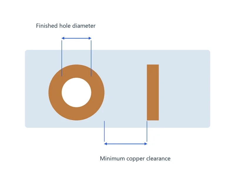
Dimensional Requirements to Specify
| Feature | Define in the drawing | Inspection basis |
|---|---|---|
| Plated and non-plated holes | Finished diameter and upper and lower limits, with PTH and NPTH identified. | Required finished condition, location and measurement method; plating and finish affect the opening. |
| Slots and internal openings | Finished width, length, end geometry and plating status. | Measure the specified geometry; slot width and overall length are separate dimensions. |
| Board outline | Finished profile dimensions and the required edge condition. | Identify routed edges, scored edges and the condition after separation. |
| Hole and profile location | Datums and coordinate or geometric position requirements. | Use the stated reference system; hole size does not establish hole position. |
| Finished board thickness | Nominal thickness, permitted limits and any coating exclusions. | Agree where and how thickness is measured and whether the evidence is from a board or coupon. |
| Layer registration | Required relationship between identified layers and features. | Specify the relevant layer pairs and the inspection or coupon method. |
Use Units and Limit Notation Consistently
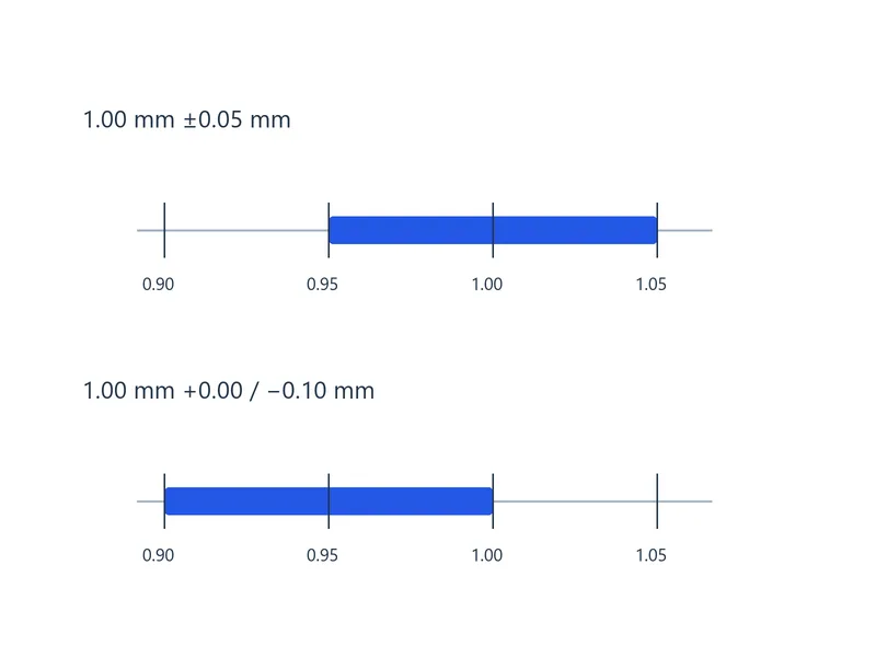
A 1.00 mm feature specified as ±0.05 mm has limits of 0.95 mm and 1.05 mm. Its total tolerance range is 0.10 mm, not 0.05 mm.
The limits 1.00 mm +0.00/−0.10 mm instead permit 0.90 mm to 1.00 mm. State units and upper and lower limits clearly, especially when a drawing combines metric dimensions and inch-based notes.
Define Copper, Electrical and Flatness Requirements
- Finished line width and gap: Nominal geometry, allowed variation, copper thickness and critical locations. Define the measurement basis for the conductor cross-section; artwork dimensions are not a complete inspection instruction.
- Surface and hole-wall copper: Required thickness, minimum or average basis, locations and sampling. A minimum copper thickness is a lower acceptance limit, not a symmetric dimensional tolerance.
- Controlled impedance: Target, tolerance, routing layer, reference layers and measurement requirements. For a 50 Ω target, ±10% means 45–55 Ω; it is an electrical range rather than a dimensional tolerance.
- Bow and twist: Applicable maximum limits, board condition and measurement procedure. These are flatness-related limits and should not be written as a general ± size tolerance.
Review Mating Features as a Combined Fit
A board can meet its drawing and still fail to fit an enclosure if the mating-part limits were not considered together. Review the board outline, mounting holes, connector locations and enclosure features against a consistent datum system.
For press-fit or locating features, provide the component drawing and required finished dimensions. We review the hole, plating and final finish together rather than applying a general hole tolerance to every connection.

Published Tolerance References
- Routed profile: ±0.005 in (±0.127 mm) Custom PCB routing reference; identify the profile dimensions and datums in the drawing.
- Finished board thickness: ±8% Custom PCB reference; specify the nominal thickness, construction and measurement basis.
- Controlled impedance: Standard ±10%; advanced ±5% Fabrication capability tiers; identify targets, stack-up and required measurement coverage.
Routing, scoring, drilling and lamination affect different features and require different controls. Specify the delivered condition, including whether a dimension applies before or after panel separation and surface finishing.
We review critical requirements alongside the broader PCB fabrication capabilities. Our custom PCB manufacturing service supports drawing-specific construction and tolerance reviews.
Prepare a Reviewable Tolerance Package
- Approved fabrication drawing, units and revision
- Board outline and drill data consistent with the drawing
- Critical feature sizes, upper and lower limits, and measurement datums
- Material, stack-up, copper and final surface-finish requirements
- Mating-part drawings for connector, mounting and enclosure interfaces
- Applicable acceptance documents, measurement methods, sampling and report requirements
Identify which dimensions control the fit or electrical function. If a proposed limit or design change is needed, we resolve it with you before manufacturing release and plan the required inspection and test records.
PCB Manufacturing Tolerance FAQs
Identify the affected feature and send the approved drawing with its revision. We review the requirement and resolve differences with the quotation and manufacturing specification before production. Do not assume a website value automatically replaces a drawing limit, or that a tighter drawing limit has been accepted without review.
Either can define a clear requirement if the units and permitted limits are unambiguous. Use a unilateral tolerance or explicit limits when the feature must not exceed one side of the nominal size. Check the resulting upper and lower sizes and avoid giving conflicting limits for the same feature.
Compare the actual board and enclosure measurements with both sets of permitted limits. Check the datums, connector locations, corner radii and any edge burrs or coatings that affect the fit. If both parts meet their drawings but interfere, review the combined tolerance stack and approve any revised interface dimensions before the next build.
No. Diameter tolerance controls the size of the opening; position requirements control where it is relative to specified datums. Identify the coordinate or geometric tolerance convention. A diametral position zone is not interchangeable with independent plus-or-minus X and Y limits.
Use the requirements in the connector manufacturer’s drawing for the finished hole range, hole-wall copper and final finish. Identify the hole group, relevant datums and inspection method in the drawing. Review the finished condition after plating and finishing; the production drill diameter alone does not define the press fit.
Identify and hold the affected boards, then record the feature, measured value, board or lot identity and drawing revision. Confirm the units, datum, finished condition and measurement method with suitable calibrated equipment. Review the result against the approved limits and agree on disposition; any authorized correction requires verification before release.
Discuss Your Critical PCB Dimensions
Send your fabrication drawing, board files and mating-part requirements. We will review the critical tolerances, manufacturing route and required verification before production.