 Skip to content


Multilayer PCB Stack-Up
Layer structures, material choices and engineering review before PCB production.
Plan Your Layer Structure Before Routing
We support multilayer PCB stack-up planning and manufacturing review for prototype and production orders. Send your proposed structure, or share the layer count, board thickness and electrical requirements so we can review a suitable build.
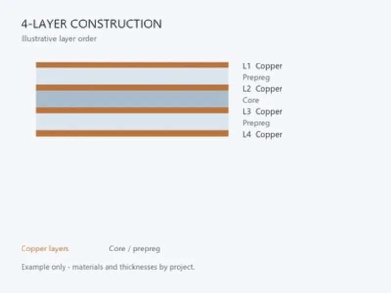
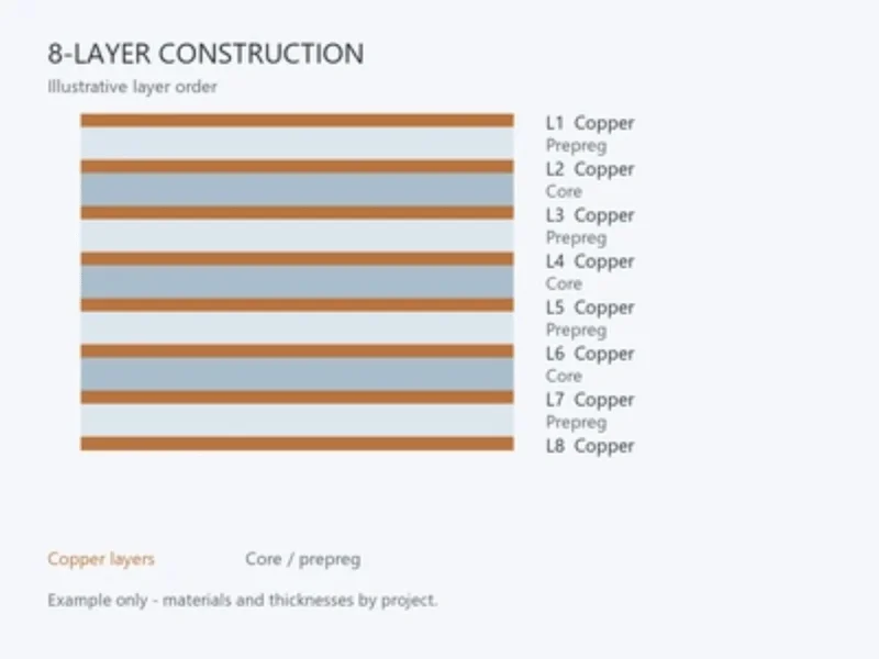
A stack-up defines the sequence of copper layers and dielectric materials through the board thickness. The layer diagrams show example constructions. We confirm the materials and dimensions for your project before production.
What Makes Up a Multilayer PCB
Copper, cores and prepreg each have a different role in the structure.
Copper Layers
Define the routing, power and reference-plane layers in the required sequence. Identify the corresponding fabrication file for every copper layer.
Cores
A core is a cured laminate that can carry copper on both sides. Specify the material system and distinguish dielectric thickness from any copper included in the quoted core thickness.
Prepreg
Prepreg bonds the layers during lamination. Its pressed thickness depends on the selected material, resin content, copper pattern and manufacturing process.

Balance Routing, Planes and Board Thickness
Adding layers creates more options for routing and reference planes. The layer arrangement depends on signal requirements, power distribution, return paths and the total board thickness.
We review the copper thickness and dielectric spacing together. Six-layer boards with the same overall thickness can use different internal constructions.
Share the critical nets, reference layers and impedance targets before finalizing trace widths. This helps align the layout with a manufacturable stack-up.
Define the Parameters That Control the Build
Provide fixed requirements and identify the choices that our engineering team can review.
Layer Sequence
List every copper layer from top to bottom, its intended function and its data file name. Include the via connections between layers.
Materials and Dielectric Spacing
Specify any required laminate grade and the pressed dielectric thicknesses. For electrical calculations, identify the dielectric constant (Dk), data source, frequency and test method. Include dissipation factor (Df) requirements where dielectric loss matters.
Copper Thickness
Distinguish starting foil from finished copper and identify inner and outer layers separately. Copper thickness affects both the manufacturing review and impedance calculations.
Finished Board Thickness
State the required overall thickness and tolerance. Make clear whether any separate mechanical dimensions refer to the dielectric, copper or the complete finished board.
Controlled Impedance
Provide target values, tolerances, signal layers, reference planes and critical geometries. Agree on the calculation and any coupon or test-report requirements.
Review Higher Layer Counts and Via Structures
For high-layer-count and HDI boards, we review the stack-up with the drilling and interconnect plan. Identify through holes, blind or buried connections and microvia layer spans.
We support conventional and sequentially laminated structures. The via structure, materials and layer arrangement help determine the manufacturing sequence. Layer count alone does not define it.
See our sequential lamination and stacked-via services for the related manufacturing process. Keep the approved layer structure and via drawing under the same design revision.
Check the Structure for Manufacturing
We review the complete material and copper arrangement before confirming the build.
Copper Distribution and Balance
Review copper coverage and the arrangement around the board centerline. Balanced construction helps control bow and twist. Special asymmetric designs need a separate review.
Resin Fill and Dielectric Control
Copper thickness and pattern density affect the resin needed between layers. Review prepreg selection and pressed spacing with the actual design data.
Material Compatibility
For mixed-material or RF constructions, identify the material grades and bonding requirements. Review electrical, thermal and processing compatibility together.
From Requirements to an Approved Stack-Up
Confirm the manufacturing structure before locking the layout and production files.
Send the Design Inputs
Share the layer count, dimensions, thickness target, materials, impedance requirements and via structure. Include any proposed stack-up and fixed customer specifications.
Review the Proposed Build
We review the material and dielectric arrangement with the copper and manufacturing requirements. Discuss any changes affecting trace geometry or electrical performance with your design team.
Approve the Production Revision
Confirm the agreed stack-up and corresponding fabrication files before release. Material substitutions, changed dielectric spacing or revised via spans need a new review.
Files for a PCB Stack-Up Review
Send your existing stack-up drawing or the requirements available so far.
- Layer count, board outline, quantity and delivery target
- Proposed layer sequence and fabrication data, when available
- Finished board thickness and tolerance
- Material grades, dielectric requirements and substitution restrictions
- Inner and outer copper requirements
- Impedance targets, reference layers and critical trace geometry
- Drill files, via layer spans and inspection or reporting requirements
Our PCB fabrication services cover manufacturing review through production. If the layout is still in development, mark which requirements are fixed and which can be adjusted.
Multilayer PCB Stack-Up FAQs
Yes. Send the layer count, board dimensions, thickness target, quantity and known material or impedance requirements. Include preliminary fabrication data if available. We can review a proposed construction for quotation, then agree on the final structure before production.
No. Boards with the same layer count and total thickness can have different copper, core and prepreg arrangements. Provide the material, copper and electrical requirements so the internal spacing can be defined. Approve the resulting layer structure before using it as the basis for controlled-impedance routing.
Yes, but review the effect on impedance, trace geometry, via construction and mechanical requirements first. Send the current layout, original stack-up and proposed change. Update any affected dimensions and impedance calculations, then approve a consistent revision of the stack-up and production files.
Send it as a design reference. We review whether its materials, pressed dielectric spacing and copper requirements can be manufactured with the proposed process. If a change is needed, the electrical and mechanical effects must be reviewed before the revised structure is approved.
Use data appropriate to the selected material, construction and operating frequency, with the calculation method identified. A single generic FR-4 value is not enough to represent every build. Share the material data and current trace geometry so the design values can be reviewed with the proposed stack-up.
Review the material properties, pressed dielectric spacing, finished thickness, impedance and the manufacturing sequence affected by the change. For vias, confirm the revised layer spans and drilling or build-up requirements. Have the responsible design team approve the updated stack-up and fabrication revision before production.
Discuss Your PCB Stack-Up
Share your layer count, material requirements and design files. We will review a manufacturable stack-up with your team.