 Skip to content


HASL PCB Finish
Hot air solder leveling for solderable PCB pads, with leaded and lead-free options.
Solder-Coated Pads for Your PCB Assembly
Hot air solder leveling (HASL) coats exposed PCB copper with solder to protect the surface before assembly and provide solderable pads. We manufacture prototype and production PCBs with leaded or lead-free HASL finishes.
Send your board files, component layout and finish requirements. We review the solder alloy, pad geometry, board construction and assembly process before confirming the manufacturing specification.

Leaded and Lead-Free HASL Options
State which HASL system your board needs. The alloy affects processing and assembly compatibility, while pad shape and leveling affect the resulting surface profile.
Leaded HASL
We apply a tin-lead solder alloy for projects that specify a leaded finish. Identify the required alloy, assembly solder system and applicable product requirements on the drawing.
Lead-Free HASL
We apply a lead-free solder alloy to exposed pads and plated-hole surfaces. Tell us the alloy and material documentation your project requires.
Match HASL to the Pad Layout
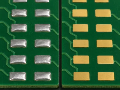
HASL is an economical option for many through-hole boards and SMT designs with larger pads. Its solder coating can support hand, wave, selective or reflow soldering when compatible with the PCB assembly process.
The coating is not uniformly flat across every pad. For fine-pitch ICs, BGA, QFN or small paste deposits, we review pad-height variation and the assembly window rather than selecting HASL by package name alone.
Where a flatter surface is needed, we can discuss ENIG or another finish alongside your PCB fabrication requirements.
How the HASL Finish Is Applied
HASL is a bare-board surface-finishing operation before component assembly. It is different from wave soldering components onto an assembled board.
Copper Preparation and Fluxing
We prepare the exposed copper and apply a compatible flux so solder can wet the intended surfaces. The board design and material system are reviewed for the finishing process.
Solder Application and Leveling
We apply molten solder and use hot-air knives to remove excess solder. Pad areas, holes and leveling conditions influence the remaining coating and surface shape.
Cleaning and Inspection
We remove process residues as required and inspect the finished board. We check solder coverage, exposed features and hole openings against the approved drawing and acceptance requirements.
HASL Specifications to Confirm
A useful HASL specification defines the alloy, functional surface requirements and inspection basis. Coating thickness can vary with feature geometry, so one nominal value does not describe every pad.
Alloy and Assembly Compatibility
Identify leaded or lead-free HASL and any specified alloy. Review the assembly solder, component restrictions and required declarations together.
Pad Coverage and Surface Profile
Specify any functional limits for coating coverage, local height or pad coplanarity. Agree the measurement locations and method when the assembly needs numerical acceptance limits.
Holes and Exposed Features
Review finished plated-hole dimensions, small openings and pad spacing after finishing. We check for excess solder that could restrict component insertion or bridge adjacent features.
Board Construction and Thermal Exposure
Review laminate, finished thickness, copper distribution and previous or planned heat cycles. We select finishing conditions for the actual board construction and material system.
Protect Solderability Before Assembly
Keep boards in their protective packaging until needed and follow the supplied storage and handling instructions. Avoid touching exposed pads or allowing moisture and contamination to reach the finish.
If boards have been stored for an extended period or the packaging has been damaged, discuss solderability verification before assembly. Appearance alone does not establish solderability, and baking should follow the board-specific instructions.
For broader material and manufacturing considerations, see our lead-free PCB manufacturing page.
Files for a HASL PCB Quote
Send the current drawing revision and identify any finish decisions that still need review.
- Gerber or ODB++ data, drill files and fabrication drawing
- Board dimensions, layer count, thickness and material requirements
- Leaded or lead-free HASL and the specified alloy, if defined
- Component layout, fine-pitch locations and critical pad or hole features
- Required coverage, surface-profile limits and inspection method
- Assembly soldering process, planned heat cycles and storage requirements
- Quantity, acceptance standard and revision, and required documentation
HASL PCB Finish FAQs
Both apply a solder coating and remove excess solder with hot air. Leaded HASL uses a tin-lead alloy, while lead-free HASL uses a lead-free solder alloy. Specify the required system and any alloy or declaration requirements so we can review assembly compatibility.
HASL can produce pad-height variation that matters for small solder-paste deposits and tight coplanarity requirements. Send the footprint, pad dimensions and assembly details for review. If the surface profile does not suit the design, we can discuss a flatter finish such as ENIG.
Send the pad layout and assembly requirements if you do not have a defined thickness limit. We can discuss suitable coverage and surface-profile requirements with you. Where a numerical limit is needed, agree the measurement locations and method before production because HASL thickness varies across different features.
No. HASL applies molten solder and levels it with hot air. Immersion tin deposits tin chemically on exposed copper. Identify the required finish explicitly in the fabrication drawing rather than specifying only a silver-colored surface.
Keep the boards in the supplied packaging and follow the specified storage conditions. Avoid pad contact, moisture and contamination. Tell us the intended storage period when ordering. If the packaging is damaged or the storage history is unclear, ask us about solderability testing before assembly.
Yes. Send the board files, intended assembly process and any lead restrictions or documentation requirements. Mark the alloy as an open decision. We can review the available options with you and confirm the selected finish before manufacturing release.
Discuss Your HASL PCB Finish
Share your board files, assembly process and finish requirements. We will review the HASL option and manufacturing details with your team.