 Skip to content


Build Copper Connections Through the Board
We provide PCB copper plating services as part of prototype and production fabrication. We form conductive connections on prepared hole walls and build copper thickness to the specified board requirements.
Send your stack-up, drill files, copper requirements and quantity. Identify critical hole groups, minimum hole-wall copper thickness and finished-hole dimensions so we can review the plating route and inspection plan together.
Establish Conductivity Before Building Copper Thickness
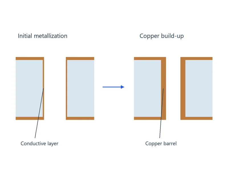
Drilling exposes dielectric material at the hole wall. We use suitable hole preparation and metallization to establish a conductive surface before electrolytic copper build-up.
The metallization route can use electroless copper or an appropriate direct-metallization process. Material, hole geometry and the required construction guide the process selection.
Specify Surface Copper and Hole Copper Separately
| Requirement | What to define | Why it matters |
|---|---|---|
| Outer-layer finished copper | Required finished thickness or copper weight for each layer. | Finished surface copper includes the starting foil and the effects of plating and material-removal processes. |
| Hole-wall copper | Minimum and any required average thickness in micrometres, with the applicable measurement basis. | A surface copper weight does not specify the copper thickness inside a hole. |
| Hole groups and layer spans | Through holes, blind or buried connections and the layers they connect. | Different geometries can need different manufacturing and verification routes. |
| Finished hole size | Diameter limits after plating and the relevant finishing operations. | Copper deposited on the wall reduces the remaining opening. |
| Coverage and acceptance | Applicable document, revision, class where relevant, and requirements for voids, interfaces and local thickness. | Thickness alone does not describe every aspect of a plated connection. |
| Inspection records | Required locations, sampling, measurement method and report format. | Results need to be traceable to the specified feature and delivered board. |
Account for Copper Distribution and Hole Geometry
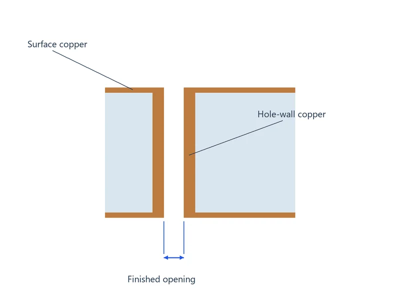
Board thickness, hole diameter and local copper distribution affect how copper is deposited on the surface and inside holes. Meeting a wall-thickness requirement must be considered alongside surface build-up and the remaining hole opening.
We review high-aspect-ratio holes and dense or uneven patterns with the complete stack-up. Where the design needs a change, we discuss the hole geometry, copper pattern or construction before releasing production data.
Coordinate Panel and Pattern Plating with Circuit Formation
Panel plating builds copper across exposed panel surfaces and hole walls. Pattern plating uses an imaged resist to limit deposition to exposed circuit features and holes in the selected process route.
These routes must be coordinated with imaging, etching and the required final geometry. We review both surface copper and hole-wall requirements rather than choosing a process from copper weight alone.
For thicker finished conductors, see our heavy copper PCB manufacturing service.
Verify the Plated Connection with the Right Evidence
Microsection inspection can evaluate hole-wall copper thickness, coverage and connection interfaces at the selected locations. Specify the sampling and any required thermal conditioning or additional reliability tests with the acceptance requirements.
Electrical testing checks connectivity and isolation under its agreed conditions. A passing electrical result does not replace the specified plating inspection; confirmed nonconformances are held for disposition and verification of any authorized correction.

Distinguish Plating, Via Filling and Surface Finishes
- Conformal copper plating: coats the hole wall while leaving an opening.
- Copper filling: fills the specified via cavity using a suitable process for that geometry.
- Resin filling and copper capping: fill the via with resin and add the specified copper cap.
- Final surface finish: protects exposed copper or provides the required soldering, bonding or contact surface.
Identify the required via construction explicitly. A plated hole is not automatically filled or capped, and a final finish does not replace the structural copper barrel.
Files for a Copper Plating Review
- Gerber or ODB++ data, NC drill files and the approved board revision
- Stack-up, materials and layer-by-layer finished copper requirements
- Hole types, layer spans and finished diameter limits
- Hole-wall minimum and any average thickness requirements, with the measurement basis
- Press-fit, via-filling or copper-capping requirements for identified features
- Acceptance criteria, inspection sampling and required records
We coordinate copper plating with our PCB fabrication services and the agreed inspection and electrical tests.
PCB Copper Plating FAQs
No. Outer-layer copper weight describes the surface conductor, not the barrel thickness. Specify the required hole-wall thickness separately, including whether it is a minimum or average value and where it is measured. We review the surface and hole requirements together before production.
State the minimum and any average requirement from the applicable drawing or specification. Include the relevant hole groups, measurement locations and sampling basis. An average can conceal a thinner local area, so it should not replace a required local minimum.
Yes. Copper deposited on the wall reduces the remaining opening. Provide the required finished-hole limits and the connector drawing so we can plan the production opening and plating allowance. Evaluate the finished fit after the specified surface finish, not from drill-tool diameter alone.
Send the board thickness, hole sizes, materials, layer spans and wall-thickness requirements. We review deposition inside the holes alongside surface copper and finished-hole limits. If the combination is unsuitable, discuss a larger hole, a different stack-up or a shorter layer span while preserving the intended connections.
No. Conformal plating creates a conductive wall and normally leaves an opening. Copper filling requires a process intended to fill the specified cavity. Mark the affected via groups and state whether the requirement is wall plating, copper fill, resin fill or a filled-and-capped pad structure.
Review the measurement and defect against the applicable plating requirements, and identify and hold the affected lot for disposition. A continuity pass does not override a failed thickness or coverage requirement. Investigate the cause and agree on further sampling, replacement or an authorized correction, followed by the required verification before release.
Discuss Your Copper Plating Requirements
Send your stack-up, hole details and copper thickness requirements. We will review the surface and hole-wall specifications, finished-hole limits and required inspection records with your PCB order.