 Skip to content


Rigid Circuit Regions with Integrated Flexible Connections
We manufacture rigid-flex PCBs that combine rigid circuit regions and flexible interconnections in one board. We support prototype and production projects, with engineering review of the regional stack-up, materials, interconnects and installed geometry.
Send your board files, flat outline and folded assembly drawing. Identify the rigid regions, flex bridges and intended movement so we can review the construction before production.
Define Each Rigid and Flexible Region
The rigid regions support components and multilayer circuitry. Selected copper layers continue through the flexible regions to form the electrical connections and allow the assembly to fit its installed shape.
A board can have six copper layers in its rigid regions and two continuing through a flex bridge. Specify the layer sequence and local thickness for each region; the total rigid-region layer count does not describe the flex construction.

Specify the Construction by Region
| Requirement | Manufacturing options or review scope | What to specify |
|---|---|---|
| Regional layers | Multilayer rigid regions with single-layer or multilayer flex interconnections | Copper-layer map and the layers continuing through each bridge. |
| Materials and bonding | Rigid laminates, flexible polyimide materials and compatible bonding systems | Material grades, adhesive requirements and permitted substitutions. |
| Local thickness | Separate rigid-region and flex-region constructions | Finished thickness and tolerance for each region, including relevant coatings. |
| Copper and impedance | Layer-specific copper and controlled-impedance structures | Finished copper by layer, conductor geometry, reference layers, impedance targets and tolerances. |
| Protection and support | Coverlay, solder mask and local reinforcement | Openings, overlap, transition boundaries and stiffener locations. |
| Interconnects | Through vias, blind or buried vias and HDI structures | Hole sizes, layer spans, filling and clearance to transition or bend zones. |
| Finish and verification | Surface finishes, electrical testing and specified construction checks | Assembly process, acceptance requirements and requested reports. |
Design the Bend Around the Actual Flex Construction
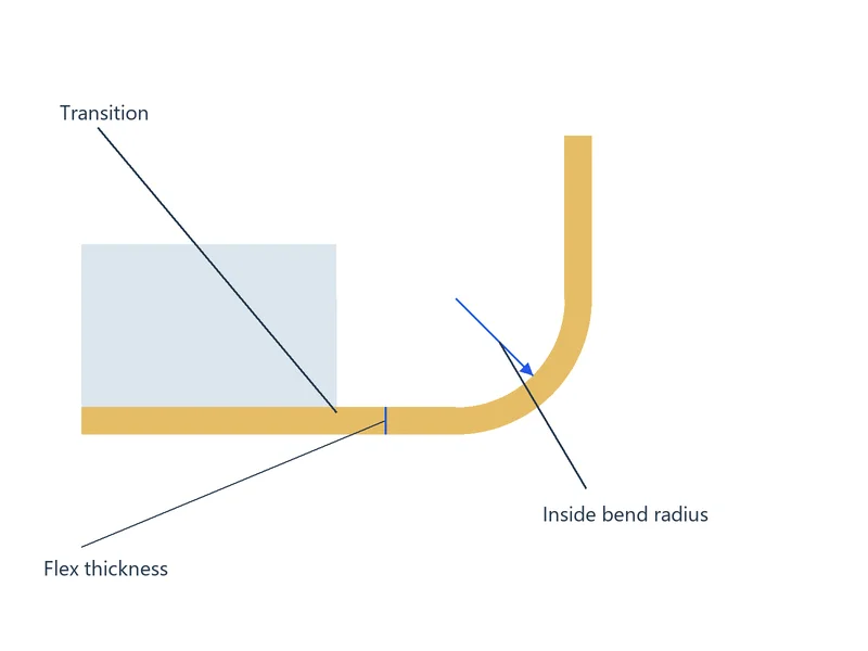
Identify whether the flex is bent during installation or moves repeatedly during use. Supply the inside bend radius, bend angle, flex length, fixed points and available enclosure space.
For repeated motion, define the required cycles, movement range, operating environment and failure criteria. We review the local flex thickness, copper distribution and materials together; a single radius multiplier does not establish fatigue life for every construction.
Review the Transition and Nearby Features
The rigid-to-flex transition needs clear boundaries for rigid buildup, coverlay, adhesive and any reinforcement. Mark keepout areas and provide the locations of holes, pads and components near each transition.
Keep bends away from abrupt thickness changes where the design allows. We review feature clearances and proposed changes against the actual construction and installed geometry before manufacturing release.
Plan Fabrication Checks and Assembly Support
Inspection can include inner-layer circuitry, regional dimensions, transition features and agreed construction checks. Electrical testing verifies the specified continuity and isolation; impedance measurements and bend qualification address separate requirements.
For assembly, specify whether the board is processed flat or formed, together with support, handling and test-access requirements. Our PCB assembly services can be quoted with fabrication.

Compare Rigid-Flex with the Other Connection Options
- Integrated rigid-flex: combines rigid circuitry and continuing flexible circuit layers in one fabricated board.
- Flex with stiffeners: adds local mechanical support without creating the same multilayer rigid circuit regions.
- Separate boards and cables: can support replacement or servicing, with connectors and assembly operations included in the comparison.
Compare the complete installed assembly, including space, connection count, support and service access. Rigid-flex can remove selected board-to-board connections, but the best architecture depends on the product requirements.
Files for a Rigid-Flex PCB Quote
- Gerber or ODB++ files, drill data and fabrication drawing
- Regional stack-ups with rigid and flex copper-layer counts
- Flat outline and installed views showing bend lines, radii and fixed points
- Materials, finished copper and local thickness requirements
- Coverlay openings, stiffeners, transition boundaries and critical clearances
- Static or repeated-motion requirements, required cycles, quantity and acceptance criteria
- BOM, placement files and support instructions when assembly is included
If the design is still developing, mark open items and send the geometry and requirements already known. Our PCB fabrication team can review the proposed manufacturing route before the final files are released.
Rigid-Flex PCB FAQs
No. A stiffener provides local mechanical support, for example beneath a connector. A rigid-flex PCB integrates rigid circuit regions with flexible circuit layers. Send the regional stack-up and component layout so we can compare the construction actually needed rather than relying on the product name.
Yes. Six copper layers can be present in the rigid region while only two continue through the flex bridge. Identify exactly which layers continue and specify the local materials, copper and finished thickness. That regional definition is needed for bend and impedance review.
Start with the required installed geometry and identify whether the bend is static or repeatedly moving. Provide the local flex construction, inside radius, angle and fixed points for review. For repeated motion, also define cycles and the environment so the required qualification can be planned. If the available radius is too small, review a thinner flex construction, fewer flex copper layers or a revised bend path before release; use the local flex thickness rather than the rigid-region thickness.
Keep vias, component pads and solder joints out of the active bend zone. For features near a rigid-to-flex transition, dimension the distance from the feature edge to the transition boundary and show the coverlay and reinforcement extents. We review those clearances with the actual stack-up and bend location, then agree on any geometry changes before production.
Yes. Send the flat outline, proposed rigid and flex layer counts, quantity and installed-space requirements. Mark the materials, thicknesses and bend details that remain undecided. We can begin the review and identify the information needed to confirm the construction and quotation.
Provide both the flat board drawing and an installed view showing the enclosure, bend lines, inside radii, fixed points and nearby components. Include the assembly sequence and any areas that must remain accessible for testing or service. We use those views to review flex length, transition placement and handling. Check the folded assembly for enclosure contact, component collisions and strain at fixed points before approving the final geometry.
Discuss Your Rigid-Flex PCB Project
Send your regional stack-up, board files and installed geometry. We will review the construction, bend requirements and fabrication or assembly scope for your order.