 Skip to content


Mixed Materials in One Multilayer PCB
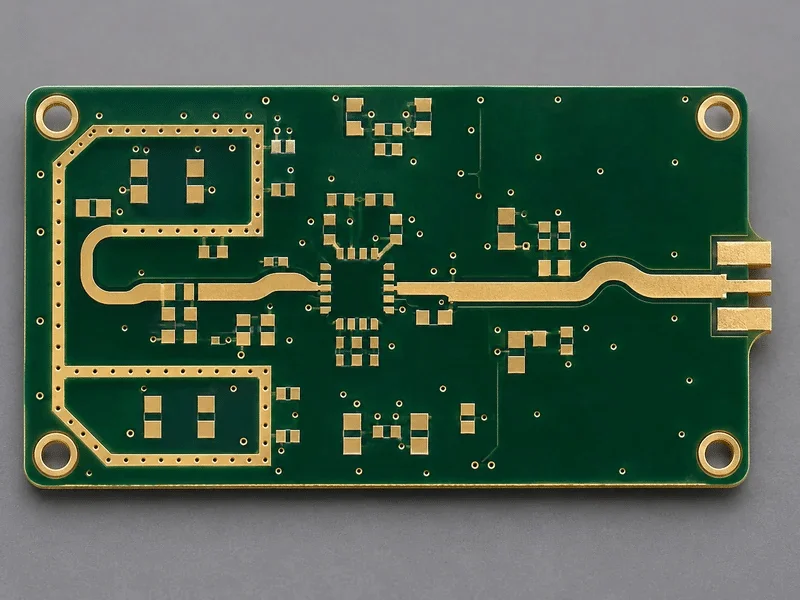
Topline Circuit fabricates hybrid PCBs that combine different dielectric materials in one multilayer board. For example, a RO4350B and FR-4 hybrid PCB can use a low-loss dielectric between an RF trace and its reference plane, with FR-4 in other parts of the stack-up where the design permits.
Send your proposed layer sequence and critical signal requirements for a stack-up review. Mark the material grades, finished thickness and electrical targets that are fixed, and tell us which details are open to change.
What to Specify in a Hybrid Stack-Up
| Parameter | What to provide |
|---|---|
| Dielectric materials | Core grades, prepreg or bondply grades, their positions in the layer sequence, and approved alternatives |
| Thickness and copper | Target finished dielectric thicknesses, finished copper thickness by layer, and overall board thickness with tolerance |
| RF and controlled impedance | Operating bands, critical nets, routing layers, reference planes, impedance targets and tolerances, and any insertion-loss limit with its test frequency or frequency band |
| Via structure | Start and stop layers, required via diameters, and any fill or cap requirements. State whether dimensions refer to the drill or the finished feature. |
| Flatness and verification | Finished-board bow and twist limits, measurement method, and any local flatness requirement under critical components |
Match the Dielectric to the Signal Path
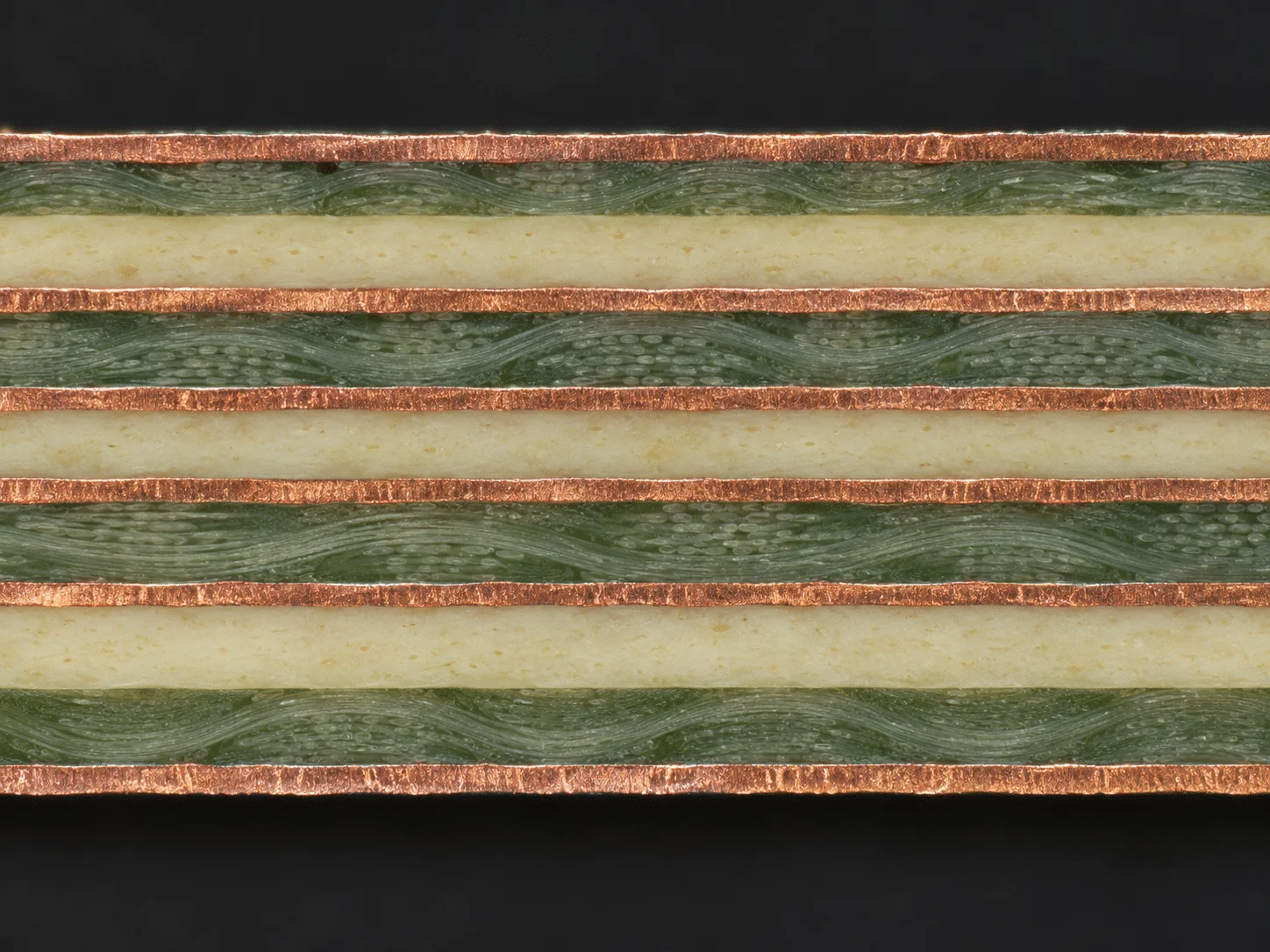
Mark the signal layer and its reference plane for each controlled trace. Identify the dielectric between them. For stripline, identify the reference planes and dielectrics on both sides of the trace.
Share the laminate grade, dielectric thickness, and copper foil requirements used in the design model. If an available material or thickness differs, recheck trace width and spacing against the impedance requirements before approving the stack-up. Include the test frequency and conditions if insertion loss must be verified.
Review Lamination and Finished Board Flatness
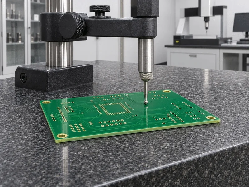
We review the core and bondply combination with the copper distribution, via spans, and finished board thickness. For an asymmetric build, provide any bow and twist limits or assembly flatness requirements so they can be considered before tooling.
If a specified core or bonding material changes, review its effect on the electrical model and finished dimensions. Record the approved PCB stack-up revision on the fabrication drawing. If you need coupon testing, specify which trace structures the coupons should represent and what the report should include.
Files for a Hybrid PCB Quote
- Gerber or ODB++ data, drill files, fabrication drawing, and layer order for the same revision
- Stack-up with the required Rogers materials or other laminate grades, thicknesses, and bonding materials
- Critical nets and reference layers, electrical targets, mechanical limits, and required test reports
- Build quantity, approved material alternatives, and any requirements still open for review
Hybrid PCB FAQs
For a preliminary quote, send the layer count, finished board thickness, quantity, and RF routing and reference layers. If the laminate grade or dielectric thickness still needs to be selected, flag it as open. Confirm the exact core and bonding materials and finished dielectric thicknesses before releasing the board for fabrication.
Yes, if the proposed stack-up can meet the flatness requirements. Send the layer sequence, copper distribution, board outline, and bow and twist limits. If a large package also needs local flatness, identify that area and its limit. Review whether the core or bonding thicknesses need to change before freezing the layout.
Ask for the replacement grade and proposed finished dielectric thickness, even if the replacement is from the same product series. Recheck impedance and any specified insertion loss on the affected traces. Confirm board thickness, then update the trace geometry and coupon design if needed. Approve the revised stack-up before fabrication.
It can. Ask for two quotes at the same quantity and with the same electrical, mechanical, and inspection requirements. Compare material cost, any additional lamination steps, and testing. Choose between the two once both proposed stack-ups meet the critical signal requirements.
Discuss Your Hybrid PCB Stack-Up
Send the proposed layer sequence, critical nets, and build quantity. Include any fixed laminate grades, finished thickness limits, or reports you need in the quote.