 Skip to content


Choose a Format for Your PCB Fabrication Files
Submit Gerber artwork with matching drill data or a complete ODB++ export. Include the fabrication drawing for requirements such as finished thickness, surface finish and controlled impedance. If your workflow uses IPC-2581, ask us to confirm the export before release.
PCB Fabrication File Formats Compared
| Format | What it carries | What to check before sending |
|---|---|---|
| Gerber RS-274X or X2 | Layer artwork. Gerber X2 can also carry attributes that identify the function of each layer. | Include matching drill and applicable routing data, and clearly identify the board profile and copper layer order. |
| ODB++ | A structured manufacturing dataset that can include layers, drill and routing features, and design attributes. | Verify that the export contains the intended board or panel, the correct layer order, the board profile and the hole data. Send the complete archive. |
| IPC-2581 | An XML-based exchange format that can include stack-up, geometry and manufacturing data. | Confirm that we can use your export version and that the file contains the data required for the build. |
Build a Complete Fabrication Package
Include all copper layers in stack-up order, solder mask and silkscreen layers as applicable, and a closed board outline with internal cutouts. Supply machine-readable drill and routing data for applicable holes and slots. Identify plated and non-plated holes and slots. Specify finished hole and slot dimensions and tolerances where critical, and give the start and stop layers for blind or buried vias.
Use the fabrication drawing to specify the stack-up, material, finished board thickness (mm), copper thickness by layer (µm or oz/ft²) and surface finish. Mark any critical dimensions and tolerances, and include impedance targets (ohms), tolerances and the layers or traces to which they apply when applicable.

Overlay the Artwork, Drills and Outline
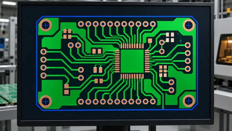
Open the exported files together in a manufacturing-data viewer. Check the finished board dimensions, layer order and orientation, then confirm that drill hits align with the intended pads and that slots and cutouts appear in the correct locations.
If drill holes shift or appear at the wrong scale, check the export units, coordinate origin, numeric format and zero suppression settings. Correct the source export and repeat the overlay check.
Identify the Files Approved for Production
Label the archive with the board part number and revision. List the fabrication drawing and the dataset approved for production, and identify any extra exports supplied for reference.
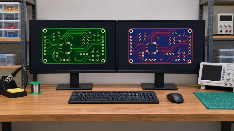
If two exports disagree, compare them against the released design and resolve the discrepancy before authorizing fabrication. Re-export affected files together so the drawing, outline and drill data match.
Submit Your PCB Fabrication Files
Put the approved files in one ZIP for upload and include the quantity and any special manufacturing requirements in your request. If you include ODB++, keep its exported archive intact.
See our PCB fabrication services for build options and our PCB DFM review for help checking the production data.
PCB File Formats for Fabrication FAQs
Check for a closed board outline with cutouts, machine-readable drill and slot data, and the fabrication drawing. If you only exported a drill map, export the NC drill data and verify it in the viewer. Identify plated and non-plated holes and slots.
If the entire drill pattern is shifted, check whether the drill and Gerber exports use the same coordinate origin. If the pattern or hole diameters appear at the wrong scale, check the units and, where applicable, the coordinate precision and zero suppression. Reopen the corrected export and verify a known hole diameter and pad alignment.
Include the approved drawing when it defines requirements for the build, such as tight tolerances, impedance, finish or acceptance criteria. Check the ODB++ archive for the correct board or panel, layer order, outline, holes and slots.
Check both exports against the released CAD revision and fabrication drawing. Resolve the differences and identify one approved production dataset in the submission. Keep the approved dataset and matching drawing in the production ZIP. If engineering needs the other export for comparison, label it as reference only and send it separately.
Ready to Submit Your PCB Files?
Send your fabrication dataset, drawing and order quantity. Tell us which files govern the build and flag any details you need us to review.