 Skip to content


Hard Gold PCB Plating
Selective hard gold for PCB fingers and wear-resistant contacts.
Hard Gold for PCB Contact Surfaces
We manufacture PCBs with selective hard gold plating for edge connector fingers and other specified contact areas. Hard gold contains alloying additions that increase hardness. Electroplated over a nickel underlayer, it provides a wear-resistant surface for mating and sliding contacts.
Send your PCB files, connector drawing and plating requirements. We review the contact geometry, nickel and gold thickness, and plating connections before confirming the manufacturing specification.
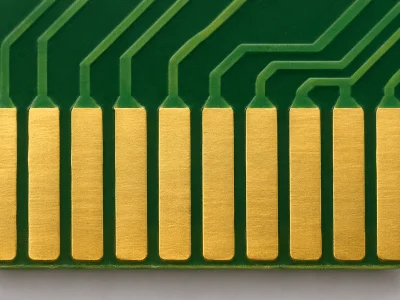
Where Hard Gold Is Used
Define the contact function first. The finish, thickness and geometry need to suit the mating interface.
Edge Connector Fingers
Gold-plated contacts along the PCB edge connect the board to a mating socket. Match the finger dimensions, board thickness and bevel to the connector drawing.
Sliding and Spring Contacts
Specified contact areas can use hard gold where repeated mechanical contact is expected. Include the mating material, contact force and operating environment when defining the finish.
Selective Plating
Apply hard gold to the defined contact regions and specify the required finish for solder pads elsewhere. We review masking, finish boundaries and the manufacturing sequence together.
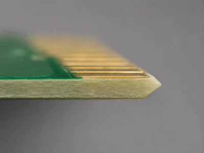
Match the Gold Fingers to Your Connector
We review the gold fingers against the finished board edge and mating connector. Board thickness, finger position and bevel geometry affect how the contacts engage.
- Finger width, spacing, length and position
- Finished board thickness and tolerances
- Bevel angle, depth and remaining edge thickness
- Outer- and inner-layer copper clearance from the routed or beveled edge
- Short or staggered fingers, key slots and contact areas on each side
Provide the connector part number or drawing with your manufacturing files. We review these details as part of our PCB fabrication services.
Specify the Nickel and Gold Layers
Put the coating requirements on the fabrication drawing. We review the requested ranges, plated area and inspection scope before quotation.
Gold Thickness
Specify the required gold thickness and units. Identify the local minimum within the functional contact area and any maximum limit. If a nominal value is given, include its tolerances and the measurement locations.
Nickel Underlayer
Define the nickel thickness separately from gold. The nickel layer supports the coating system and acts as a barrier between copper and gold.
Hardness and Contact Conditions
Include any required hardness, deposit composition and acceptance standard. Share the expected mating conditions so the plating specification can be reviewed against the application.
Units and Drawing Notes
Use consistent units for each layer. For example, 30 µin equals 0.762 µm. Select the required thickness using the connector specification and contact conditions.
Plan Selective Plating with the Board Layout
Plating access and panel construction affect the manufacturing route. Include isolated contact pads and unusual edge features in the engineering review.
Electrical Access for Plating
Electroplating needs a conductive path to each plated feature. We review temporary plating buses or tie bars, including how they connect to the contact area.
Masking and Finish Boundaries
Mark the hard gold regions on the drawing. Define where the contact finish ends and where the solderable finish begins, including any areas that must remain unplated.
Routing and Connection Removal
The production plan must account for removal of temporary connections and edge finishing. The finished board must retain the intended contact geometry without unintended electrical connections.
Plated Area and Quotation
Gold thickness and plated area affect material use. Masking, plating access, panel layout and inspection requirements also affect the quote. Mark the functional contact regions clearly so we can review the scope.
Choose Hard Gold for the Contact Interface
Hard gold is an electroplated contact finish selected for wear resistance. ENIG uses a thin immersion-gold layer over electroless nickel and is primarily a solderable finish.
Soft gold serves different requirements, including qualified bonding applications. Select the deposit properties for the intended use. Confirm soldering or wire-bonding requirements separately before using hard gold on those pads.
For boards with both contact fingers and solder pads, specify the finish for each region. We can review this alongside your PCB assembly requirements.
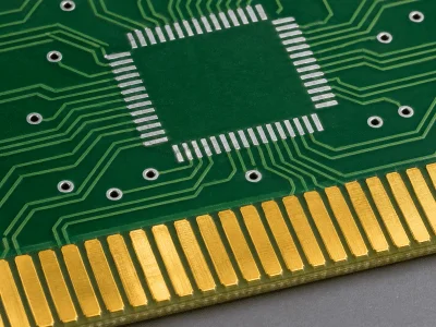
Inspection for the Specified Contact Area
We review the inspection requirements with your drawing so the finished contact regions can be checked against agreed criteria.
Contact Geometry and Appearance
Review the finished fingers, bevel, surface coverage and visible defects against the approved drawing. Confirm the condition of the contact area and the board edge.
Coating Thickness
Agree on the measurement method, locations and sampling for nickel and gold. A thickness report should identify the measured areas and the acceptance limits.
Additional Verification
Specify any required adhesion, porosity or contact-performance testing before production. Define the method, sampling and acceptance criteria with the order.
Files for a Hard Gold PCB Quote
Send the current manufacturing files and mark the hard gold regions clearly.
- Gerber or ODB++ data, drill files and fabrication drawing
- Board material, layer count, dimensions and finished thickness
- Gold finger details, connector drawing and bevel requirements
- Separate nickel and gold thickness requirements with units
- Required hardness, finish boundaries and finish for other pads
- Inspection criteria, sampling and report requirements
- Order quantity and applicable drawing revision
Hard Gold PCB Plating FAQs
Hard gold is electroplated for contact areas that need wear resistance. ENIG provides a thin immersion-gold layer over electroless nickel and is primarily used for solderable pads. Identify which areas will be soldered and which will make mechanical contact so we can review the finish for each region.
Use the connector specification or your qualified contact requirements as the starting point. Specify nickel and gold separately, with units, acceptance limits and measurement locations. If the coating requirements are not defined, send the connector details and operating conditions for review before releasing the drawing.
Yes. We can review selective hard gold on the fingers with a separate finish for the solder pads. Mark both finish regions and their boundaries on the drawing. Include any isolated contact pads so we can plan the required electrical connections for plating.
Use the requirements of the mating connector. Send its part number or mechanical drawing, together with the finished PCB thickness and tolerances. We review the bevel angle, depth and remaining edge thickness against those requirements.
Electroplating needs an electrical path to the area being plated. Temporary buses or tie bars provide that path during manufacturing. We review their placement and removal so the finished PCB has the intended contact dimensions and electrical connections.
Cycle life depends on gold thickness, contact force, wiping distance, the mating surface and the environment. A thickness value alone does not establish a cycle rating. Provide the connector rating or required test conditions so the coating specification and any verification testing can be agreed.
Discuss Your Hard Gold PCB Requirements
Share your board files, connector drawing and plating specification. We will review the manufacturing and inspection requirements with your team.