 Skip to content


ENIG PCB Finish
Electroless nickel immersion gold for flat, solderable PCB pads.
Flat Gold-Finished Pads for PCB Assembly
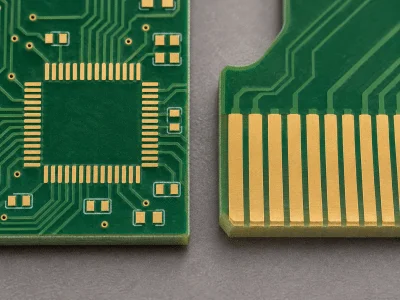
We manufacture prototype and production PCBs with electroless nickel immersion gold (ENIG) finishes. The nickel layer forms a barrier over copper, while the thin gold layer protects the nickel before assembly. Together, the layers provide a flat, solderable finish.
ENIG offers a flat pad surface for fine-pitch layouts, BGA and QFN packages. Send your board files, nickel and gold thickness requirements, and assembly details so we can review the finish specification for your design.

The Nickel and Gold Layer Structure
ENIG is a two-metal finish over the PCB copper. The nickel and gold layers have different functions and must be specified and measured separately.
Electroless Nickel
A nickel-phosphorus layer is deposited on the prepared copper. It acts as a diffusion barrier. During soldering, the thin gold layer dissolves into the solder. The nickel layer reacts with the solder to form the joint interface.
Immersion Gold
A thin gold layer is deposited over nickel by a chemical displacement process. It protects the nickel surface before assembly. Its role differs from the thicker hard-gold coating used for repeated sliding contacts.

Plan ENIG Around Your Pad Layout
A flat finish helps control solder-paste deposition and component seating in dense layouts. We review exposed pad geometry, solder-mask openings, via treatment and assembly requirements for fine-pitch ICs and area-array packages.
ENIG avoids the raised solder coating associated with HASL. Finish selection still needs to account for the package land pattern, paste printing and the planned PCB assembly process.
For RF designs, include any surface-finish restrictions in the fabrication notes so the nickel layer can be considered in the electrical design review.
ENIG Thickness and Specification
Specify nickel and gold thickness separately, in micrometers (µm). Use the ranges below for initial review and confirm the production limits on the approved drawing.
Nickel Thickness
A reference range for the electroless nickel layer is 3–6 µm. State the required range and acceptance basis on the fabrication drawing so we can confirm the production specification.
Gold Thickness
Define the immersion-gold thickness separately from nickel. A reference range is 0.065–0.10 µm. We confirm the selected range against your ordered specification and the finish process.
Measurement and Records
Specify measurement locations, sampling and any required thickness report. Calibrated X-ray fluorescence (XRF) can measure the nickel and gold layers using a method suitable for the coating system and pad geometry.
Board and Acceptance Requirements
Include material, finished thickness, pad and hole features, and the required standard revision. If IPC-4552 is required, state its revision and any customer-specific acceptance requirements.
Choose the Finish for the Interface
Solder pads, edge contacts and wire-bond pads have different requirements. Choose the coating system for how each surface will be used.
ENIG and HASL
ENIG provides a flatter metallic pad surface. HASL applies a solder coating and can be economical for compatible through-hole and larger-pad designs. Compare the finish with the actual assembly requirements.
ENIG and Hard Gold
ENIG is primarily a solderable finish. Repeated mating and sliding contact can require electroplated hard gold, with thickness, hardness and contact geometry specified for the application.
ENIG and ENEPIG
ENEPIG adds a palladium layer between nickel and gold. For wire-bonded designs, select the finish using the wire material, bonding process and qualification requirements rather than treating the finishes as interchangeable.
Verify the Finish Beyond Its Appearance
We review nickel and gold coverage, thickness requirements and the inspection records needed for your build. Process control is important because nickel corrosion associated with black pad can affect solder-joint integrity.
Surface appearance alone does not establish thickness, solderability or the condition of the nickel interface. Specify any additional solderability or interface evaluation with the order so the verification plan can be agreed before production.
Keep boards in their protective packaging and follow the supplied storage instructions. For wider manufacturing considerations, see our lead-free PCB manufacturing page.
Files for an ENIG PCB Quote
Send the current drawing revision with the ENIG requirements marked in the fabrication notes.
- Gerber or ODB++ data, drill files and fabrication drawing
- Board dimensions, layer count, material and finished thickness
- Separate nickel and gold thickness ranges, units and measurement locations
- Critical pad geometry, via treatment and assembly requirements
- Any RF, wire-bonding or repeated-contact requirements
- Acceptance standard and revision, sampling and required reports
- Order quantity and any storage or packaging requirements
See our PCB fabrication services for the wider manufacturing scope.
ENIG PCB Finish FAQs
No. ENIG uses a thin immersion-gold layer over electroless nickel to provide a solderable finish. Hard gold is an electroplated contact finish used where wear resistance is required. Tell us whether the area will be soldered, probed or repeatedly mated so we can review the appropriate finish.
Specify the two layers separately, including units, required ranges and the acceptance standard revision. Reference ranges are 3–6 µm for nickel and 0.065–0.10 µm for gold. Confirm the required ranges against your ordered specification. If you have not defined the ranges, send the pad layout and assembly requirements for review before the drawing is released.
Yes. Its flat pad surface can suit BGA, QFN and fine-pitch layouts. Include the footprint, solder-mask openings and via details so we can review the finish alongside solder-paste printing and assembly requirements.
Black pad is associated with excessive nickel corrosion during ENIG processing. We review the required process-control records and verification plan with your order. Thickness measurement alone does not rule out this issue. Tell us if solderability testing or interface evaluation is required, so we can agree on the method, sampling and acceptance criteria before production.
Suitability depends on the wire material and bonding process. Send those details with your qualification requirements. We can compare ENIG, ENEPIG and other finish options against those requirements. Bond performance must be verified through the agreed qualification process.
Yes, when included in the agreed inspection scope. State the required nickel and gold values, measurement locations, sampling and report format before production. Include any board or lot identification needed for your traceability records.
Discuss Your ENIG PCB Requirements
Share your board files, nickel and gold specifications, and assembly requirements. We will review the finish and inspection scope with your team.