 Skip to content


Choose the Right Surface Treatment for Each Via
Topline Circuit supports open vias, soldermask tenting, via plugging and filled-and-capped constructions for prototype and production PCBs. We review the required surface condition with your via geometry, nearby pads and assembly process.
Tell us which vias need coverage, which must remain accessible and which form solderable component pads. We help turn those requirements into a clear manufacturing specification.
Covering the Opening Is Different from Filling the Hole
Tenting places a soldermask film over a via opening. Plugging introduces material into part of the hole. Filling places material throughout the via cavity, while copper capping forms a metal surface over a filled via.
These treatments produce different surfaces. Specify the required result and the treated side rather than relying on the word covered alone.

Compare the Via Covering Options
| Option | Result | Selection point |
|---|---|---|
| Open via | The hole remains open and the specified copper land is exposed through a soldermask opening. | Preserve required solder or probe access; review interaction with nearby solder joints. |
| Tented via | Soldermask spans the opening without intentionally filling the barrel. | Review hole size, mask application and required coverage; a tent is not a copper pad. |
| Plugged via | Plugging material occupies part of the hole from the specified side or sides. | Define the material, plugging extent and any additional soldermask coverage. |
| Filled via | Specified filling material occupies the via cavity. | Define fill acceptance and the required final surface; filling alone does not specify a copper cap. |
| Filled and covered | A filled via has an additional soldermask covering on the specified surface. | Use where the surface needs mask coverage, with any required test access identified separately. |
| Filled and copper-capped | The filled via has a metallized copper cap. Specify the finish and soldermask opening where the cap must remain solderable. | Specify a solderable surface where the via is part of a component pad. |
Match Via Covering to the Pad and Assembly Process
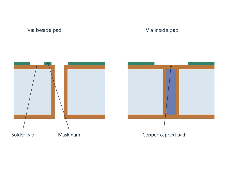
A via beside a solder pad and a via inside that pad need different reviews. Check whether a soldermask dam can separate an adjacent open via from the solderable land.
Where a via inside a component pad needs a continuous solderable surface, specify filling, planarization and copper capping. For the material and process options, see our filled via manufacturing services.
Specify the Required Coverage
- Via groups: identify the holes receiving each treatment. Keep component lead holes and required mounting openings out of the treatment groups unless the drawing explicitly specifies otherwise.
- Treated sides: mark top, bottom or both sides for tenting, plugging or secondary coverage.
- Geometry: identify production drill size and plated-hole diameter before filling, board thickness, via-pad dimensions and clearance to nearby solderable lands.
- Material and construction: distinguish soldermask, plugging material, resin fill and copper cap.
- Surface acceptance: state required coverage, permitted openings or pinholes, fill criteria and planarity where relevant.
- Assembly and finish: identify the surface finish, reflow exposure and package-specific requirements.
Keep Test Access and File Outputs Consistent
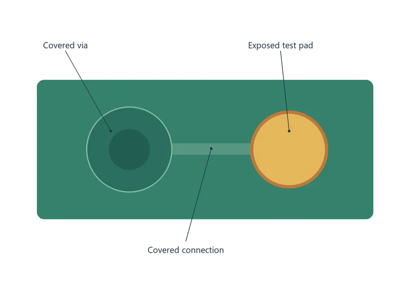
A covered via cannot automatically serve as an exposed probe point. Mark the lands that need electrical test or inspection access and specify their soldermask openings and finish.
Keep the top and bottom soldermask layers, drill files, via map and fabrication notes consistent. Omitting a soldermask opening does not by itself request resin filling or copper capping.
Review Coverage with the Manufacturing Process
We review the selected treatment with hole size, board thickness, mask application, filling material and curing process. Coverage and surface requirements are checked against the approved fabrication drawing.
Where internal fill quality or copper-cap construction matters, specify the required inspection method and records. Visual coverage alone does not establish the internal condition of a filled via.
Files for a Via Covering Review
- Gerber or ODB++ data, including top and bottom soldermask layers
- Drill files and a fabrication drawing
- A via map or separate identification of each treatment group
- Side-specific covering, plugging, filling and copper-capping requirements
- Test points, component lead holes and other features that must remain open
- Surface finish, acceptance requirements, quantity and relevant assembly details
Our PCB DFM review checks the treatment callouts against your production data before manufacturing.
PCB Via Covering FAQs
First check the exported top and bottom soldermask layers, not only the CAD display setting. Removing a mask opening requests coverage but does not specify complete filling or guarantee a closed tent. Hole size and mask application affect the result. If closure is required, define the permitted opening and the required plugging or filling construction in the fabrication drawing.
No. A tent spans the opening, while a plug extends into part of the hole. Specify the treated side, plugging material and extent if a plug is required. Add any secondary mask covering separately rather than assuming the terms describe the same structure.
For a nearby via, check whether the pad and via can be separated by a manufacturable soldermask dam. For a via inside a solderable BGA pad, specify the filled-and-capped surface required by the land pattern and assembly process. A soldermask plug is not a substitute for that copper surface.
Only if the required contact surface remains accessible. Identify probe locations and provide suitable exposed lands, mask openings and finish. If the via must stay covered, add a separate accessible test pad instead of relying on the probe to pierce the soldermask.
Yes. Identify each group and the top and bottom treatment in a via map or fabrication drawing. A side-specific covering callout does not by itself define how far a plug or fill extends into the hole. Specify that construction separately and match it to the mask and drill outputs. Resolve conflicting instructions before approving the production data.
Separate the affected boards and compare the observed condition with the approved coverage requirements. Record the locations, photos and assembly thermal profile if reflow has occurred. Review exposed copper, loose mask and nearby joints before deciding on acceptance, qualified repair or replacement; do not cover the defect with unapproved ink.
Review Your Via Covering Requirements
Send your board files and identify the surfaces that need protection, solderability or test access. We will review the treatment groups and prepare a manufacturing quotation.