 Skip to content


Multilayer Boards for Your Design Requirements
We manufacture rigid multilayer PCBs for prototype and production orders. Our services combine engineering review, material selection, inner-layer processing, lamination, drilling, copper plating and final inspection.
Send your board files, quantity and proposed layer count. We review the stack-up, finished thickness, copper requirements and interconnect structure together before confirming the manufacturing specification.
Choose Layers for Routing, References and Power
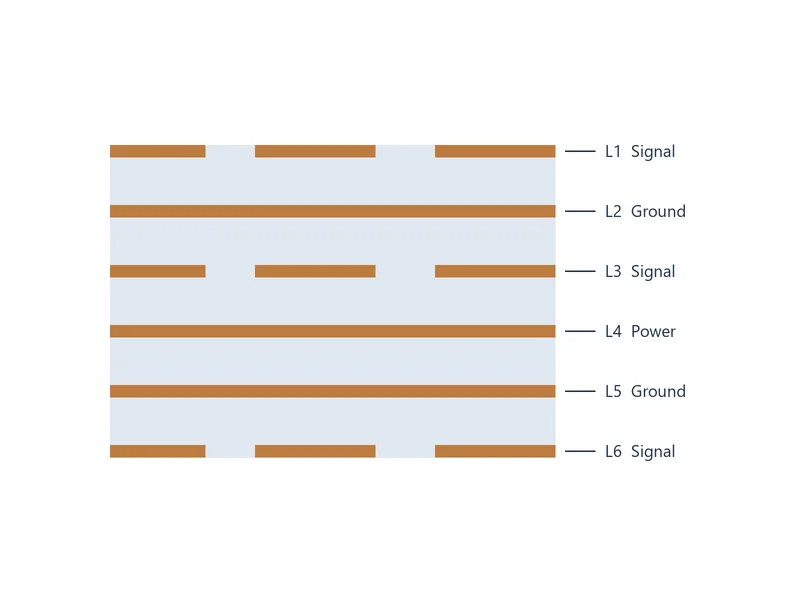
We support rigid multilayer builds up to 40 layers. Common starting points include 4, 6, 8 and 10 copper layers, with the construction selected for the design requirements. Choose the construction around component escape, board area, continuous signal references and power distribution.
More layers provide additional routing and plane options. Signal integrity still depends on the layer arrangement, return paths, materials and interconnect geometry; layer count alone does not establish electrical performance.
Define Your Multilayer PCB Specification
| Requirement | Available options or review scope | What to provide |
|---|---|---|
| Layer count | Rigid multilayer builds up to 40 copper layers | Required copper-layer count and proposed layer roles. |
| Materials | FR-4, high-Tg and application-specific material systems | Exact grade where required, permitted alternatives and thermal requirements. |
| Thickness and copper | Custom stack-up, finished board thickness and layer-by-layer copper | Thickness limits, finished copper and critical dielectric spacing. |
| Interconnects | Through holes, blind and buried vias, and HDI structures | Finished hole sizes, layer spans, filling and capping requirements. |
| Controlled impedance | Single-ended and differential structures | Target, tolerance, layer, reference planes and verification requirements. |
| Surface finish | Lead-Free HASL, ENIG, ENEPIG, OSP, immersion silver and immersion tin | Selected finish, coating specification and assembly requirements. |
| Verification | Inner-layer inspection, electrical testing and specified construction checks | Acceptance requirements, sampling and requested shipment records. |
Review the Physical Stack-Up Before Layout Release
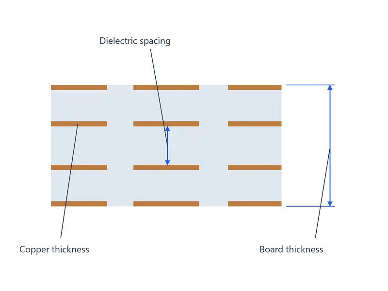
A layer-role list is the starting point. The manufacturing stack-up also needs material grades, core and bonding constructions, pressed dielectric spacing and finished copper thickness.
For controlled-impedance PCBs, we review those values with conductor width, spacing and reference planes. Identify any dimensions or materials that cannot change so proposed adjustments can be approved before production.
Match the Via Structure to the Build
Through vias connect through the full board thickness. Blind and buried vias connect selected layers, while HDI constructions can use microvias to support dense component escape.
The via layer spans, hole dimensions and board thickness affect the fabrication route. Our HDI PCB manufacturing service covers related build-up requirements; specify filling, copper capping and any backdrilling in the fabrication package.
Inspect Internal Circuits Before They Are Enclosed
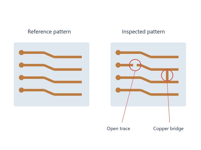
Inner-layer circuits are patterned and inspected before lamination. The approved construction then guides bonding, drilling, hole metallization and the remaining outer-layer processes.
Electrical testing checks the specified continuity and isolation requirements. Microsections and impedance measurements address different questions, so identify the required checks and report scope during quotation rather than treating one test as proof of every board property.
Compare Equivalent Builds When Reviewing Cost
- Layer count and size: compare the routing benefit of added layers with board area and panel use.
- Material and copper: keep laminate grades and finished copper requirements consistent between quotations.
- Via structure: compare the same drill sizes, layer spans, filling and lamination stages.
- Finish and verification: include the same coating, electrical test and reporting requirements.
We can review proposed changes with you before quoting a revised construction. Changes to material, dielectric spacing or copper geometry need to preserve the electrical and mechanical requirements.
Files for a Multilayer PCB Quote
- Gerber or ODB++ files with an unambiguous copper-layer order
- Drill files, hole chart and fabrication drawing
- Proposed stack-up, material grades and finished board thickness
- Finished copper requirements and controlled-impedance details
- Via layer spans, filling, capping and backdrilling instructions
- Board dimensions, quantity, surface finish and required test records
If the stack-up is not final, mark the open items and send the requirements already known. Our PCB fabrication team can review the proposed construction; PCB assembly can also be included in the quotation.
Multilayer PCB FAQs
Compare component escape, routing density, continuous references and power distribution within the same board outline. Identify which constraint the extra layers solve. Send your placement, critical interfaces and proposed layer map so we can review the manufacturing implications of the candidate constructions.
Yes. Send the proposed layer count, board dimensions, finished thickness, material requirements, quantity and any impedance targets. Mark unknown values clearly. We can begin the review with those requirements, then confirm the construction and any quotation changes before manufacturing release.
Not necessarily. Total thickness depends on the selected cores, bonding layers and copper, not just the number of copper layers. State the finished thickness and tolerance required by the enclosure or connector. We review available constructions together with drill geometry and dielectric spacing.
No. Through vias are suitable for many multilayer designs. Consider blind vias, buried vias or microvias when component escape, routing space or electrical requirements justify them. Provide the required layer spans and component pitch so the interconnect structure can be reviewed before choosing a more complex build.
Review the replacement before approving it. The material properties and pressed dielectric spacing can change the impedance, even if the nominal board thickness stays the same. Identify affected layers and targets, update the stack-up and approve any required geometry changes before production.
Compare the full specification rather than the layer count alone. Check material grades, board size, finished copper, drill sizes, via filling, surface finish and required verification. Send both sets of assumptions for review so differences in scope can be separated from differences in price.
Discuss Your Multilayer PCB Project
Send your board files, proposed stack-up and quantity. We will review the materials, interconnects and verification requirements for your prototype or production order.