PCB board technology is how modern electronics get both mechanical support and copper interconnects on a single laminate—pads, traces, vias, layers, and materials that determine density, speed, heat, and cost. By the end of this introduction, you should be able to tell what a board is made of, which construction types fit which projects, and what to lock before you compare fabrication or assembly quotes.
Hardware teams and procurement readers still need that shared vocabulary when they evaluate suppliers. The sections below move from definition and anatomy to stack-up, materials, board types, and the fab-versus-assembly split—so engineering and purchasing can align on requirements before fabrication starts.
What a PCB actually is
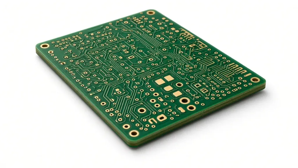
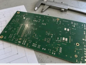
A printed circuit board (PCB) is a flat laminate that provides mechanical support for electronic components and copper interconnects that route electrical signals between them. Pads, traces, and vias replace the hand-soldered wires that once linked discrete parts point to point. That shift cut assembly time, reduced wiring errors, and made repeatable, high-density designs practical for production.
In short: the board holds the parts in place and connects them through patterned copper. Without that dual role—structure plus interconnect—modern electronics would still depend on bulky wire harnesses and one-off chassis wiring.
Anatomy of a modern board
A finished bare board is a stack of functional layers, not a single sheet of plastic with copper on top. Understanding each layer helps when you read a fab drawing or a stack-up note.
Substrate (core or laminate): The dielectric base that gives the board its stiffness and electrical insulation.
Copper foil: Conductive layers etched into traces, planes, and pads.
Solder mask: The usually green (or other color) coating that protects copper and defines where solder can wet.
Silkscreen: Ink legends for reference designators, polarity marks, and assembly cues.
Pads: Exposed copper (often finished) where components solder or bond.
Vias: Plated holes or microvias that connect copper from one layer to another.
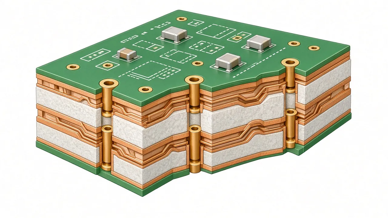
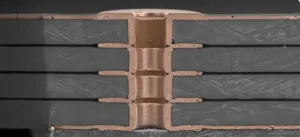
Think of the board as a sandwich: dielectric cores and prepreg “glue” layers alternate with copper foils; outer copper is covered by solder mask and silkscreen, with openings only where pads and vias must remain accessible. That sandwich description is what fabricators mean when they talk about stack-up.
Layers and stack-up
Layer count is one of the first decisions that drives cost, thickness, and electrical performance.
Single-sided boards carry copper on one face—simple, low-cost, and limited in routing density. Double-sided boards add copper on both faces, usually with plated through-holes connecting them. Multilayer boards add internal copper layers laminated between cores and prepreg, enabling denser routing, dedicated power/ground planes, and controlled return paths.
In a multilayer stack-up, a core is a rigid dielectric already clad with copper; prepreg is partially cured resin-glass that bonds cores and foils during lamination. Designers assign some layers as signal layers and others as power or ground planes. Continuous planes improve power integrity by lowering impedance of the supply network and improve signal integrity by giving high-speed traces a clear reference—topics covered in more depth on controlled impedance PCBs.
Choosing layer count is not only “more layers = more room.” Extra layers add lamination cycles, drilling complexity, and scrap risk. Match the stack-up to routing density, impedance targets, and mechanical thickness—not to a generic preference for “as many layers as possible.”
Materials that change the design
FR-4 (glass-reinforced epoxy) is the default substrate for most commercial electronics: widely available, well understood, and cost-effective for moderate speeds and temperatures. Many projects never need to leave FR-4.
When loss, dielectric constant stability, or heat change the picture, material choice becomes a design decision:
PTFE and other low-loss laminates (including Rogers-class and similar options from several suppliers) are common for RF and microwave work where insertion loss and dielectric stability matter. See PCB materials and high-frequency PCB for construction notes.
Metal-core boards (often aluminum) spread heat away from LEDs, power stages, and other hot components. Review aluminum metal core PCBs when thermal paths dominate the mechanical design.
Polyimide is the usual base for flexible circuits that must bend, fold, or survive repeated flex cycles.
An aluminum pcb is the usual metal-core construction when LEDs or power stages need a metal base to spread heat. Specify it on the RFQ rather than treating every hot design as thicker FR-4; construction details live on the aluminum metal core PCBs page linked above.
Material swaps affect drill parameters, lamination profiles, impedance calculations, and sometimes finish compatibility. Call out the laminate family early so quotes and DFM reviews use the same assumptions.
Board types you’ll meet in production
Production RFQs rarely say only “PCB.” They name a construction class. Here is when each type tends to appear, and one trade-off to keep in mind.
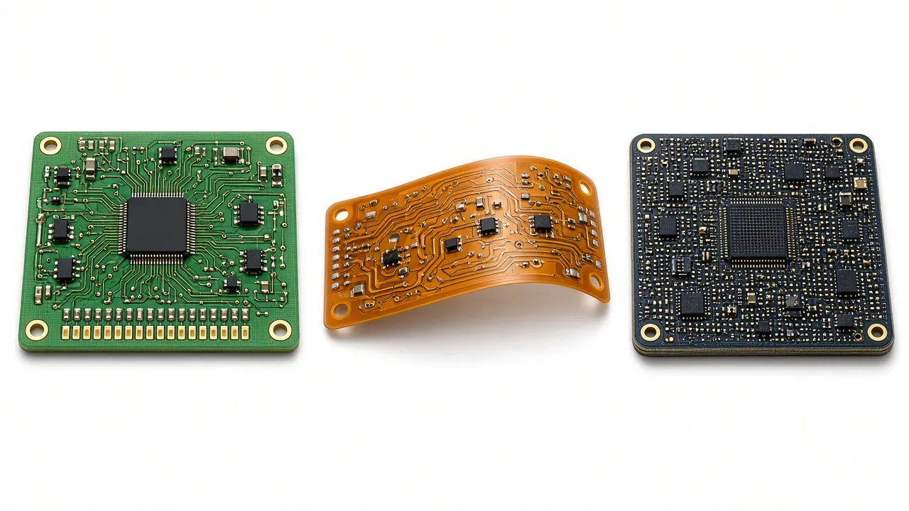
Rigid — Standard FR-4 (or similar) boards for most controllers, modules, and consumer electronics. Trade-off: excellent stability and cost, but no intentional bend; connectors or cables are needed for motion or packaging constraints.
Flex — Polyimide-based circuits that bend into tight enclosures or replace discrete wiring. Trade-off: higher material and process cost than a simple rigid board; see flexible circuits.
Rigid-flex — Rigid sections for components joined by flexible regions for 3D packaging. Trade-off: fewer connectors and better reliability in motion, at the price of more complex stack-up and tooling; details on rigid-flex PCBs.
HDI (high-density interconnect) — Microvias, finer lines, and often sequential build-up for fine-pitch BGAs and compact products. Trade-off: higher fab cost and tighter process control; justified when escape routing or size targets leave no alternative—see HDI PCB.
Heavy copper — Thicker copper foils for high current and improved thermal mass. Trade-off: etching and plating become harder as copper weight rises; plan for heavy copper PCBs when current density or heat in the copper itself is the driver.
RF & microwave — Controlled dielectric, low-loss materials, and careful stack-up for antennas, filters, and front ends. Trade-off: material cost and fab discipline rise with frequency; construction notes live under RF & microwave PCB.
Pick the type from packaging, electrical, and thermal needs—then confirm the supplier can run that construction at your volume and acceptance class.
From bare board to assembled product
Two scopes are easy to conflate in an RFQ.
PCB fabrication produces the bare board: laminate, copper patterning, drilling, plating, solder mask, silkscreen, surface finish, and electrical test of the bare circuit. Capability overviews sit on PCB fabrication.
PCB assembly places and solders components onto that bare board—SMT, through-hole, mixed technology, inspection, and often programming or functional test. That scope is covered under PCB assembly.
A complete product may need both, plus component sourcing and agreed acceptance criteria. Early builds often start as PCB prototyping so the team can validate layout and process before volume. Fabrication and assembly can be quoted together or separately; what matters is that the revision, BOM, and inspection plan stay consistent across both scopes.
This article does not walk through a manufacturing process step by step. The useful distinction for procurement and engineering is simpler: decide whether you are buying bare boards, assembled boards, or both—and state that clearly on the quote request.
What to decide before you request a quote
A complete quote request shortens back-and-forth and produces prices you can compare. Before you send files, align on:
Stack-up — Layer count, thickness targets, impedance requirements, and any blind/buried or microvia structures.
Materials — Laminate family (FR-4, PTFE/low-loss, metal-core, polyimide, hybrids) and Tg or loss goals where relevant.
Surface finish — HASL, ENIG, OSP, immersion silver/tin, or hard gold—driven by assembly process, shelf life, and fine-pitch needs.
Quantity — Prototype, pilot, and production volumes, plus expected revisions.
Acceptance criteria — IPC class, electrical test scope, impedance coupons, AOI/X-ray expectations for assembly, and documentation you need with shipment.
When those items are clear, share Gerbers or ODB++, fab notes, BOM, and placement data with a single revision tag. For a review or quotation, contact Topline Circuit with quantity, delivery target, and any open design questions.
Frequently asked questions
What is the difference between a PCB and a PCBA?
A PCB is the bare printed circuit board—the laminate with copper, solder mask, and finishes, without components mounted. A PCBA (printed circuit board assembly) is that same board after components have been placed and soldered, and often after programming or functional test. Quotes should state whether pricing covers bare boards only, assembly only, or a turnkey PCBA including parts. Mixing the terms on an RFQ is a common source of mismatched scope and price.
Why do multilayer boards cost more?
Each additional layer adds copper foil, prepreg or core material, lamination cycles, registration risk, and usually more drilling and plating work. Inner-layer imaging and inspection also scale with layer count. Multilayer boards also enable features—planes, controlled impedance, denser routing—that may require tighter process control. The higher unit price reflects materials and process complexity, not only “more copper.”
When is HDI worth using?
HDI is worth using when component pitch, board size, or routing density cannot be met with conventional through-hole vias and standard line/space. Fine-pitch BGAs, wearable and handheld designs, and modules that must shrink package outline are typical drivers. If a standard multilayer stack-up can escape the devices with through vias and acceptable thickness, HDI may add cost without benefit. Evaluate microvia structure against real escape and impedance needs, not as a default upgrade.
When should you choose flex instead of a cable harness?
Choose flex when the interconnect must bend inside a fixed envelope, survive repeated motion with fewer discrete connectors, or reduce assembly steps in a compact product. A flex circuit can replace a harness of wires and connectors with a single controlled part. Choose a cable harness when the path is long, serviceability requires disconnects, volumes are low, or flex tooling and material cost would not pay back. Rigid-flex sits between those options when components need a rigid island and a flexible link.
When is FR-4 not enough?
FR-4 is not enough when dielectric loss or Dk stability at your operating frequency hurts RF performance, when continuous high temperature exceeds the laminate’s rating, when heat must be pulled through a metal core, or when the product must flex. In those cases, move to low-loss/PTFE-class materials for RF, higher-Tg or specialty laminates for harsh thermal environments, metal-core constructions for heat spreading, or polyimide for flex. Confirm the substitute with impedance and reliability requirements before locking the stack-up.
Once stack-up, materials, finish, and acceptance criteria are clear, Topline Circuit in Shenzhen can support projects from layout through fabrication and assembly under one build definition—so engineering and procurement stay aligned from prototype to production.
Engineering Support for Your PCB Project
Need help with your PCB or assembly project? Contact our team to discuss your design, manufacturing and testing requirements.
Inconsistent solder paste deposits on fine-pitch HDI pads can result from poor paste release from the stencil, uneven board support, problems with paste storage or handling, or incorrect printer settings. The HDI
The cost of a 10-layer rigid PCB depends on its size, materials, copper weight, hole structure, and manufacturing requirements. Order quantity, testing, and delivery timing also affect the quote. Two boards with
A PCB design needs any-layer HDI when conventional HDI cannot provide the required layer connections within the available board space and thickness. This can happen with dense BGA packages, limited routing channels,
To provide the best experiences, we use technologies like cookies to store and/or access device information. Consenting to these technologies will allow us to process data such as browsing behavior or unique IDs on this site. Not consenting or withdrawing consent, may adversely affect certain features and functions.
Functional
Always active
The technical storage or access is strictly necessary for the legitimate purpose of enabling the use of a specific service explicitly requested by the subscriber or user, or for the sole purpose of carrying out the transmission of a communication over an electronic communications network.
Preferences
The technical storage or access is necessary for the legitimate purpose of storing preferences that are not requested by the subscriber or user.
Statistics
The technical storage or access that is used exclusively for statistical purposes.The technical storage or access that is used exclusively for anonymous statistical purposes. Without a subpoena, voluntary compliance on the part of your Internet Service Provider, or additional records from a third party, information stored or retrieved for this purpose alone cannot usually be used to identify you.
Marketing
The technical storage or access is required to create user profiles to send advertising, or to track the user on a website or across several websites for similar marketing purposes.
 Skip to content