Why Is Solder Paste Printing Inconsistent on Fine-Pitch HDI Pads?
Inconsistent solder paste deposits on fine-pitch HDI pads can result from poor paste release from the stencil, uneven board support, problems with paste storage or handling, or incorrect printer settings. The HDI structure alone does not explain why the deposits vary.
We recommend checking where the variation occurs and when it starts. Compare deposits immediately after printing, then use that pattern to choose the next check.
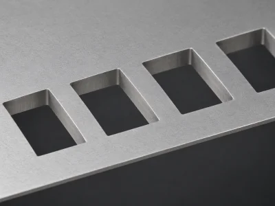
When SMT solder paste volume varies on the same fine-pitch pads across consecutive boards, inspect the solder paste stencil first: aperture area ratio, wall condition, and underside residue often explain a repeating location pattern before printer settings need to change.
1. Confirm That the Variation Starts at Printing
Inspect the paste before component placement. Printing is one stage of the PCB assembly process, so a defect found after reflow does not, by itself, prove that printing caused it.
Compare the same pad locations across consecutive boards. Keep the board revision, stencil, paste, and inspection program unchanged while establishing this baseline.
Look for a Location or Timing Pattern
Record whether the problem affects one component, repeats at the same panel position, or appears across the board. Also note whether it begins after a pause or improves after stencil cleaning.
These observations help narrow the investigation, but they do not confirm a root cause. For example, low paste volumes around one package justify checking its stencil apertures and the board support beneath it.
We recommend using the observed pattern to choose the first checks:
If the same pads have low paste volumes on successive boards, inspect their apertures and local board support.
If deposits change after a pause, review paste handling and restart conditions.
If deposits improve after cleaning, inspect the apertures and stencil underside for residue.
Save inspection images and measurements before adjusting the printer. Changing several settings immediately makes the original problem harder to trace.
2. Check Whether the Smallest Apertures Release Paste Reliably
Small openings need closer attention to stencil geometry and paste release. NPL’s research identifies aperture area ratio, wall finish, aperture design, and paste choice as important factors in ultra-fine-pitch printing. NPL research
Inspect the affected apertures for retained paste, contamination, damage, and differences from the approved drawing. Compare the actual stencil with the correct paste-layer revision.
Calculate Area Ratio Using the Actual Aperture
Area ratio compares the opening area with the area of its walls. For a rectangular opening, it is calculated as:
Area ratio = (length × width) / [2 × (length + width) × stencil thickness]
As a calculated example, a 0.20 mm square opening in a 0.10 mm stencil has an area ratio of 0.50. Reducing the thickness to 0.08 mm raises it to 0.625, but also reduces the opening’s theoretical paste volume.
This example illustrates a tradeoff, not an approved stencil design. A thinner stencil must still provide enough solder for the other components.
Review Fine-Pitch and Larger Pads Together
One stencil thickness may not suit every pad on a mixed-component board. Eurocircuits discusses step stencils as one way to provide different thicknesses in different areas. Solder paste data preparation
We recommend reviewing aperture changes with the stencil supplier and assembly engineer. Check the required solder volume before approving a design change, then evaluate the modified stencil in a controlled printing trial.
Include the component manufacturer’s recommendations in that review. A change that improves release must still suit the package and its land pattern.
3. Check Board Support and Stencil Contact
The board needs stable support during the print stroke. Inspect the support arrangement, clamping, and local flatness around the affected pads.
Also inspect the underside of the stencil for paste outside the intended openings. Review stencil contact in that area rather than assuming every local defect requires a different paste.
Board support, PCB planarity, solder mask consistency, and stencil gasketing are all listed in Indium’s printing guide as factors affecting transfer efficiency. Gasketing means the contact that helps keep paste within the intended openings. Solder printing basics
Review the Local Pad and Mask Features
Compare the actual pads and mask openings with the approved fabrication data. Include any via-in-pad features and their specified surface treatment in the review.
Do not assume that every HDI board has the same pad construction. Infineon’s package assembly guidance considers stencil thickness, PCB quality, solder mask, vias, and paste together when defining an assembly process. Infineon assembly guidance
That guidance applies to the packages it covers. Use the recommendations for your actual component when approving a land-pattern or stencil change.
4. Match the Paste to the Apertures and Handling Conditions
A finer powder can help with small-aperture printing, but powder size alone does not define a suitable paste. The flux system and reflow performance also matter.
Indium explains that finer powder has more surface area for a given solder volume. This increases the demand on the flux during reflow. Fine-powder printing and reflow tradeoffs
We would not select Type 5 or Type 6 paste simply because a board uses HDI technology. Ask the paste supplier to assess the actual aperture dimensions, stencil thickness, alloy, and assembly requirements.
Follow the Product’s Storage and Use Instructions
Check the paste lot, expiry date, storage history, and time on the stencil. Use the specific product’s instructions for conditioning, mixing, working life, and reuse.
Allow refrigerated paste to reach the specified working temperature before opening its container. Indium warns that opening cold paste can allow moisture to condense on it and affect performance. Paste handling and storage
Avoid applying a generic warming time to every container and product. Record the actual preparation steps so a material change can be separated from a printer adjustment.
5. Review Print Settings and What Happens After a Pause
Print speed, squeegee pressure, and separation settings need to suit the paste and stencil. A setting copied from another assembly is a starting point for evaluation, not evidence of a stable process.
Indium’s setup guidance notes that different pastes can respond differently to print speed. It also recommends evaluating separation behavior with attention to the smaller apertures. Printer process setup
Review the squeegee condition and whether it leaves a clean wipe. Adjust the pressure to achieve a clean wipe instead of increasing it whenever the paste volume is low.
Compare the last print before a pause, the first print after restarting, and subsequent prints. Record cleaning events separately so their effect is visible.
If deposits improve after cleaning, inspect the affected apertures and stencil underside. Treat the improvement as evidence for further checking, rather than proof that the cleaning interval was the only cause.
6. Use Solder Paste Inspection (SPI) to Compare Deposits
Solder paste inspection provides more useful evidence than a board-level pass or fail alone. Depending on the system, measurements can include volume, area, height, and shape. Koh Young’s description of 3D SPI
Compare equivalent apertures across boards and panel positions. Keep different aperture designs separate so their intended volume differences do not look like process variation.
Review the spread of the measurements as well as their average. A reasonable average can hide individual deposits that fall outside the approved limits.
Before changing those limits, confirm that the inspection program matches the board revision and stencil aperture design. Check questionable measurements against the actual deposits and the equipment supplier’s inspection guidance.
We recommend recording the following for each trial:
The affected pad locations and aperture dimensions.
Paste volume, area, and height where available.
Board sequence, panel position, and print direction.
Time since the previous print and stencil cleaning.
The single change made and its measured result.
Treat SPI results as part of the wider inspection plan, not a stand-alone pass or fail. Volume and height data are more useful when they can be compared with later AOI or X-ray findings on the same pads. See our testing and inspection notes for how those checks fit together.
7. Verify the Change Before Accepting the Process
Start with the cause best supported by the evidence. Keep other inputs fixed during a simple comparison, or use a planned experiment when several interacting factors need evaluation.
Check whether the change improves the affected deposits without creating a problem elsewhere. Include restart conditions if the original variation appeared after pauses.
Then confirm the result after placement and reflow. A more consistent print still needs to produce acceptable solder joints under the approved assembly and inspection requirements.
For an engineering review, keep the PCB data, paste-layer revision, stencil drawing, paste datasheet, printer settings, and inspection records together. This gives the engineer the design and process information needed to investigate the printing problem within the SMT assembly process.
What should we send to review inconsistent SMT solder paste printing?
Share the PCB and paste-layer revision, the solder paste stencil drawing or paste-layer Gerber, the paste product and lot notes, printer settings, and SPI images or volume data for the affected pads. Keep the board revision, stencil, and inspection program unchanged across the sample set so the comparison stays valid.
Need a printing review? See our SMT PCB assembly and testing & inspection pages. Send the PCB data, stencil file, paste details, and SPI records via Contact Us — Topline Circuit will review the pattern before recommending a process change.
Engineering Support for Your PCB Project
Need help with your PCB or assembly project? Contact our team to discuss your design, manufacturing and testing requirements.
PCB board technology is how modern electronics get both mechanical support and copper interconnects on a single laminate—pads, traces, vias, layers, and materials that determine density, speed, heat, and cost. By the
The cost of a 10-layer rigid PCB depends on its size, materials, copper weight, hole structure, and manufacturing requirements. Order quantity, testing, and delivery timing also affect the quote. Two boards with
A PCB design needs any-layer HDI when conventional HDI cannot provide the required layer connections within the available board space and thickness. This can happen with dense BGA packages, limited routing channels,
To provide the best experiences, we use technologies like cookies to store and/or access device information. Consenting to these technologies will allow us to process data such as browsing behavior or unique IDs on this site. Not consenting or withdrawing consent, may adversely affect certain features and functions.
Functional
Always active
The technical storage or access is strictly necessary for the legitimate purpose of enabling the use of a specific service explicitly requested by the subscriber or user, or for the sole purpose of carrying out the transmission of a communication over an electronic communications network.
Preferences
The technical storage or access is necessary for the legitimate purpose of storing preferences that are not requested by the subscriber or user.
Statistics
The technical storage or access that is used exclusively for statistical purposes.The technical storage or access that is used exclusively for anonymous statistical purposes. Without a subpoena, voluntary compliance on the part of your Internet Service Provider, or additional records from a third party, information stored or retrieved for this purpose alone cannot usually be used to identify you.
Marketing
The technical storage or access is required to create user profiles to send advertising, or to track the user on a website or across several websites for similar marketing purposes.
 Skip to content