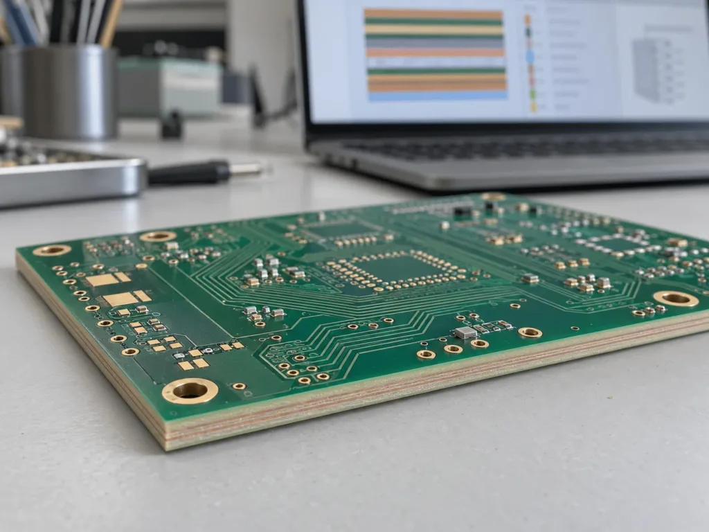
We plan the PCB stackup before detailed routing starts. We first choose the layers and reference planes, then agree on materials, copper, impedance rules, and vias with the manufacturer. We test the proposed structure against the placement before releasing it for routing.
Define What the Board Must Support
Our starting point is the circuit, the component packages, and the space inside the enclosure. We use an earlier stackup only after checking it against those requirements. A familiar layer count does not prove that the new board will fit or route.
Identify the critical signals
We list the interfaces that need controlled impedance, length matching, or separation from noisy circuits. For each one, we record the device requirements and the route from source to load. We consider signal edge rate as well as clock frequency when deciding which paths need close review.
For each critical interface, note its target impedance and whether it uses single-ended traces or differential pairs. Identify any restrictions on layer changes or via stubs. Keep these requirements available when choosing the signal layers.
Record package and mechanical constraints
Review the pin pitch, pad arrangement, and escape options for BGAs and dense connectors. Check the board outline, connector positions, and thickness limits at the same time. These details determine where routing space is available.
A connector may set the finished board thickness. A dense package may need smaller vias or more signal layers. We separate these fixed limits from preferences so that a proposed change does not alter the board’s fit or function.
Estimate the Layer Count From Routing Space
We treat the first layer count as a working estimate. We test the difficult package escape, major interfaces, and power paths before choosing every dielectric thickness. This early check shows whether the proposed layers can do their assigned jobs.
Try the difficult routes first
We use a preliminary placement to test the densest BGA escape and the narrowest routing corridor. The test uses trace widths, clearances, and via sizes that the manufacturer can support. If it depends on an unconfirmed feature, we keep that route unresolved.
Separate routing congestion from poor placement. Moving a connector or rotating a component may release enough space without adding layers. If the critical routes still cannot fit with their spacing and reference requirements, revise the layer count or via plan.
Matched buses and differential pairs need more space than a simple net count suggests. Include room for pair spacing, separation from other signals, and any required length adjustment. This makes the estimate more useful than counting connections alone.
Assign a role to every layer
Our layer map names the job of each copper layer: signal, ground, power, or mixed use. It also names the reference plane for every critical signal layer. We then check the space left for general routing and power distribution.
A separate plane is not required for every power rail. Some rails can use copper regions or traces sized for their current and voltage-drop limits. Reserve dedicated planes where the electrical and physical requirements justify them.
Choose Reference Planes and Layer Order
We choose each critical signal layer together with its reference plane. We follow the planned route over that plane, including connector areas, cutouts, and dense via fields. Available routing space is useful only if the required return path remains intact.
Keep critical routes over continuous copper
Avoid taking a critical route across a split, slot, or void in its reference plane. The interruption forces the return current away from the signal path. Change the route or plane arrangement before committing to that layer assignment.
Two adjacent signal layers also need attention when long traces run parallel on them. Their coupling depends on the spacing and surrounding structure. A plane between them can reduce that interaction, but the final arrangement must still meet the board’s routing and thickness needs.
Plan the return path at layer changes
When a signal changes between layers that reference separate ground planes, provide a nearby ground connection between those planes. Review where a return via can fit beside the signal transition. Do not wait until routing is complete to find that the required connection has no space.
A transition between different reference nets needs a different review. A ground via cannot connect a power plane to ground without creating a short. Check the interface guidance and the required high-frequency return connection before using that transition.
Altium’s high-speed design documentation explains return-path checks and plane transitions. Use those principles with the actual reference nets and device requirements. A generic via rule cannot cover every interface.
Check construction balance
We ask the manufacturer to compare dielectric spacing and copper thickness on opposite sides of the board’s center. We also flag large differences in copper coverage between paired layers. A symmetric drawing can still contain uneven copper distribution.
Balance does not require identical routing patterns on every layer. It requires a construction review that considers the materials and copper arrangement. Keep any approved exception in the fabrication notes.
Set Material and Impedance Requirements Together
We choose the material and trace geometry together. If the material changes, we check whether the old impedance calculation still applies. We update the CAD rules before routing against a different construction.
Specify the material properties that matter
We compare material options with the circuit’s loss, thermal, and mechanical requirements. If an approved laminate is mandatory, we record its exact designation and the substitution policy. A general FR-4 note cannot communicate that restriction.
Check the frequency and test method behind a quoted dielectric constant. Different data-sheet values should not be treated as interchangeable inputs. Ask which value the manufacturer will use for the proposed impedance calculation.
Use finished construction values
Ask for the proposed core and prepreg arrangement and the finished dielectric thicknesses used in the model. A nominal prepreg value alone does not define the pressed distance between copper layers. The proposal should also show how the complete structure meets the finished board thickness.
State whether copper requirements refer to starting foil or finished copper. Outer-layer plating can change the copper thickness and trace profile. Those finished assumptions belong in the impedance model, not only in a purchasing note.
Define each controlled routing class
Our impedance requirements name the target, tolerance, routing layer, reference plane, and material assumptions. We add the proposed trace width and pair spacing for each relevant class. We agree which dimensions the manufacturer may adjust before accepting the construction.
Our article on stackup factors that affect controlled impedance explains these relationships. Use the approved values to create the CAD routing rules. If a dielectric or copper value changes, recalculate before continuing with the old geometry.
Match the Via Plan to the Stackup
We plan vias while the layer arrangement is still open to change. Each via type needs defined start and stop layers. Its construction must support package escape without taking away the routing space we need elsewhere.
Choose via types for an identified need
Test whether through vias support the package escape without blocking the inner routing channels. If they do not, review blind vias, buried vias, or microvias with the manufacturer. Compare the available routing space with the added construction requirements.
Record the exact layer span for each proposed via type. Do not infer the number of lamination cycles from overlapping spans alone. The manufacturer must establish the sequence from the drilling method, subassemblies, and required interconnections.
For stacked or staggered microvias, include the proposed arrangement in the review. Filling, plating, and the connection between stages are part of the construction. A simple line between two layer names does not fully specify it.
Review stubs on sensitive routes
A through via can leave unused copper beyond the layer where the signal exits. Review that stub against the interface requirements and channel model. Depending on the structure, a different routing layer, blind via, or backdrilling may be appropriate.
Altera’s high-speed signal layer planning notes discuss these choices for FPGA transceivers. Treat the examples as device-specific guidance rather than a requirement for every board. The chosen solution must also fit connector and manufacturing limits.
Check the Proposal Against Placement and Power
We test the stackup against the preliminary placement before detailed routing. This connects the layer plan with the practical checks in our PCB layout process. We start with the difficult areas, where a failed assumption can affect the rest of the board.
Confirm that the escape routes use the proposed trace and via rules. Follow critical routes across connectors and layer changes to check their references. If a necessary route crosses a plane interruption, resolve it in the placement or stackup.
Review power paths for narrow copper necks, blocked connections, and excessive route length. Check how each load and its decoupling capacitors connect to power and ground. Use the current and voltage-drop requirements to judge those paths rather than assuming that any copper region is sufficient.
Approve One Stackup Revision Before Routing
Our review package includes the layer order, material requirements, copper definitions, and finished thickness. It also includes impedance classes and via spans. We mark fixed limits and acceptable alternatives so that the construction proposal can resolve the remaining choices.
Send the same revision the manufacturer will use for impedance modeling: layer order, materials, finished thicknesses, and each impedance class. A controlled impedance review is faster when those values are written down before routing starts. If you already have a draft table, include target impedance, layer, reference plane, trace width or pair spacing, and the dielectric values used in the calculation.
Review changes before accepting them
We compare the proposal with all the design requirements. We check material substitutions, dielectric distances, finished copper, and via construction. If a change affects trace geometry or package escape, we repeat the relevant routing check.
Resolve the critical unknowns before detailed routing begins. A suitable placeholder in an early plan is not an approved production value. Record who must confirm each open item and which routing decisions depend on it.
Release matching documents and CAD rules
We release the same approved revision in the stackup drawing, fabrication notes, and CAD layer settings. Our impedance profiles and via rules must match that revision. We keep the approval record as the reference for any later change.
Before release, we check that each critical route has enough space, a suitable reference, and an allowed layer transition. We also check that the manufacturer has confirmed the materials and construction. Any unresolved item stays visible in the release record instead of becoming an assumed production value.
FAQ
What should a PCB stackup review package include?
Layer order and copper definitions, material callouts, finished thickness, via spans, and each controlled-impedance class with its reference plane. Mark what is fixed and what the fabricator may adjust. A draft is enough for an engineering check; an unapproved placeholder should not be treated as a production value.
Want a stackup check before routing? See PCB layout and controlled impedance PCBs, then send the draft stackup via Contact Us.
 Skip to content