 Skip to content


Printed Antenna Boards Built to Your RF Design
We manufacture antenna PCBs for prototype and production orders. We review the specified material, stack-up, conductor geometry and feed structure with your fabrication files.
Send your artwork, target frequency bands and installed-product requirements. Identify the radiator, ground geometry and critical dimensions so the manufacturing review preserves the intended RF structure.
Define the Radiator and Feed Structure
Printed antenna constructions include board-edge inverted-F and meander antennas, microstrip patches and arrays, and printed dipoles or slots. Flexible antenna boards can place the radiator away from the main electronics.
The feedline carries energy to the antenna; it is not automatically the radiating element. Specify the complete structure, including any ground or counterpoise, matching or balun network, and connection to the RF circuit.
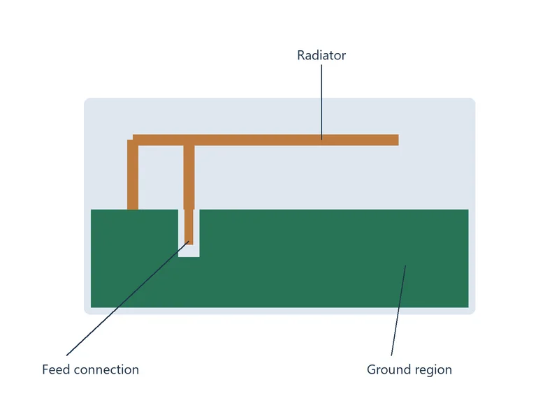
Specify the Features That Affect the RF Structure
| Requirement | Manufacturing review | What to provide |
|---|---|---|
| Frequency and antenna type | Required radiator, feed and board construction | Operating bands, architecture and approved circuit artwork. |
| Material and dielectric | Laminate grade, dielectric spacing and material substitutions | Laminate grade, design Dk and Df with their frequency and data source, plus dielectric thickness and tolerance. |
| Copper geometry | Finished copper thickness, etched features and registration | Critical lengths, widths, gaps and dimensional tolerances. |
| Feed network | Signal geometry and continuous references | Specified feed impedance and tolerance, transmission-line geometry, reference layers where applicable, and connector launch. |
| Ground and keepouts | Ground outline, slots, vias and specified clearances | Layer-by-layer copper, component and mechanical keepouts. |
| Mask and surface finish | Coating coverage and specified metal finish | Mask openings, coating requirements and approved finish. |
| Verification | Fabrication acceptance and separately defined RF measurements | Inspection, test method, limits, reference plane and required records. |
Match Materials and Stack-Up to the Antenna

Some compact printed antennas use FR-4 successfully. Other designs need tighter dielectric control or lower-loss materials, depending on frequency, bandwidth, geometry and efficiency requirements.
Our high-frequency PCB manufacturing service covers related low-loss constructions. Approve changes to material, dielectric spacing, copper or mask coverage against the antenna design before releasing the revised build.
Preserve the Ground and Installed Clearances
Ground size, slots and keepout areas are part of the antenna design. Define them on every affected layer instead of copying only the visible radiator shape.
Provide the position of the enclosure, battery, cables, connectors and nearby metal. These features can change antenna behavior, so evaluate the final installed configuration when tuning or qualifying the product.
Separate Board Checks from Antenna Validation
Fabrication inspection checks the specified conductor pattern, dimensions and construction. Electrical continuity testing and feedline impedance measurements address different requirements from antenna matching and radiation.
Define any required S11 or VSWR measurements separately from gain, radiation pattern and efficiency measurements. Agree on the fixture, measurement conditions, installed configuration and report scope before quotation. Define the calibration reference plane for port measurements; a matched input alone does not establish radiation performance.

Plan Matching and Assembly Before the Prototype
Provide the matching-network footprints, component values and connector details with the assembly files. Keep measurement access and any approved tuning provisions consistent with the RF layout.
Our PCB assembly services can be quoted with fabrication. Record prototype tuning changes in the artwork and BOM revision so repeat builds use the approved configuration.
Files for an Antenna PCB Quote
- Gerber or ODB++ artwork, drill data and dimensioned fabrication drawing
- Frequency bands, antenna architecture and critical geometric tolerances
- Material grade, layer stack-up, finished copper and dielectric requirements
- Ground outlines, layer-by-layer keepouts, mask openings and surface finish
- Feed impedance, connector launch and matching-network details
- Enclosure or installation drawings showing nearby metal and components
- Quantity, acceptance requirements and requested fabrication or RF reports
- BOM and placement data when assembly is included
If the antenna layout is still developing, identify the open design questions. We can review the available files for manufacturing, while antenna design approval and the required RF validation remain defined in the project scope.
Antenna PCB FAQs
Not always. FR-4 can suit some printed antennas, while other designs benefit from lower loss or tighter dielectric control. Compare the actual frequency bands, bandwidth, efficiency target and board geometry. Provide the reference design and material requirements before substituting a laminate.
Preserve the complete reference construction, including board thickness, material, ground dimensions, keepouts and feed geometry. Copying the copper silhouette alone can change the result. Review any differences, then tune and verify the antenna in the intended installed product.
First check the populated matching parts and connector assembly against the BOM and layout. Then check the ground, keepouts and nearby metal, and measure the installed antenna across the required bands. Feedline impedance alone does not establish antenna matching, efficiency or the performance of the complete radio link.
No. A good input match does not show how much accepted power is radiated or in which direction. Specify gain, efficiency and radiation-pattern measurements where those properties matter. Compare results using consistent measurement conditions and the specified installed configuration. For port measurements, define the calibration reference plane and account for fixture and cable effects.
Compare measurements before and after installation with the same setup. Check the battery, cables, metal parts and enclosure spacing against the design. Review those physical changes before adjusting the matching network or approved antenna geometry. Verify the revised installed assembly across the required bands and update the released artwork and BOM.
Yes. Send the available artwork, outline, quantity, proposed materials and target bands. Mark critical dimensions and unresolved items clearly, and state whether the request is for fabrication, assembly or additional RF validation. We can identify the manufacturing information needed to confirm the quotation.
Discuss Your Antenna PCB Project
Send your antenna artwork, material specification and installation requirements. We will review the manufacturing scope and the inspection or validation records needed for your order.