 Skip to content


Ceramic Circuits for Thermal and Electrical Requirements
We provide ceramic PCB manufacturing for prototype and production orders. We review the ceramic material, conductor process and assembly requirements together to define the construction for your circuit.
Send your artwork, dimensioned drawing and quantity. Include heat-load, insulation and joining requirements so we can review the substrate, metallization and inspection scope before production.
Choose the Ceramic for the Application
Alumina (Al₂O₃) is a starting point for many ceramic circuits. Compared with many alumina grades at the same thickness and area, aluminum nitride (AlN) can reduce substrate thermal resistance. Silicon nitride (Si₃N₄) is used in power substrates where mechanical and thermal-cycling requirements affect material selection.
Compare the actual material grade, thickness, electrical properties and metal-to-ceramic system. For RF circuits, include operating frequency and dielectric requirements rather than choosing the substrate by thermal conductivity alone.

Match the Circuit Process to the Design
| Process | How the circuit is formed | Selection requirements |
|---|---|---|
| DPC — Direct Plated Copper | A deposited adhesion and conductive seed system supports patterned copper plating. | Fine features, plated copper thickness, adhesion, holes and surface finish. |
| DBC — Direct Bonded Copper | Copper is directly bonded to a suitable ceramic substrate and patterned. | Power-circuit geometry, copper thickness, spacing and thermal cycling. |
| AMB — Active Metal Brazing | An active braze joins copper and ceramic. | Ceramic and braze system, copper layout and reliability requirements. |
| Thin film | Thin metal layers are deposited and patterned. | Precision geometry, metal stack, electrical properties and bond surfaces. |
| Thick film | Compatible conductor or functional pastes are printed and fired. | Paste system, conductor geometry and any resistor or overcoat requirements. |
| LTCC / HTCC | Patterned ceramic tape layers and compatible conductors are laminated and co-fired. | Internal layers, vias, firing shrinkage, cavities and package dimensions. |
Review the Complete Heat Path
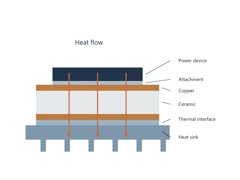
Substrate conductivity is only one part of thermal design. Ceramic thickness, heat-source footprint, copper layout, attachment layers and the interface to the cooler all affect the temperature rise.
Provide the power dissipated as heat, source dimensions, cooling arrangement and temperature limits. We use those requirements to review the proposed construction; a conductivity value alone does not establish junction temperature or assembly performance.
Define Dimensions and Conductors for the Selected Process
- Substrate: material grade, thickness, tolerance, outline, flatness and surface requirements.
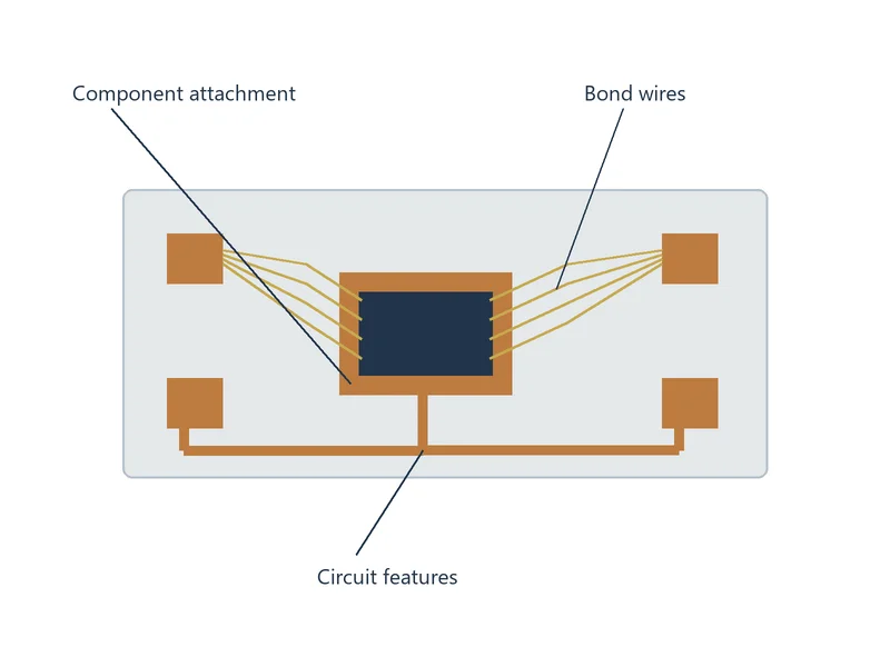
- Conductors: metal system, finished thickness, line width, spacing and critical pad dimensions.
- Holes and edges: hole type, electrical connection, edge distance and allowable edge condition.
- Interfaces: finish, joining method, bond areas and required adhesion or attachment criteria.
- Electrical acceptance: continuity and isolation limits, operating voltage, separately specified dielectric withstand tests, and any RF measurements.
We review dimensions against the selected material and process. A fine-line DPC rule and a heavy-copper DBC rule describe different constructions, so they must not be combined into one generic design limit.
Coordinate Assembly, Handling and Inspection
Identify whether the circuit will be soldered, bonded, sintered or attached by another specified method. Include the required surface finish, joining materials, thermal exposure and mechanical support.
Inspection can include circuit dimensions, ceramic condition, metal thickness and agreed electrical checks. Specify any additional qualification and records during quotation. Our PCB assembly services can be reviewed alongside the bare-substrate order.
Compare Ceramic with Metal-Core and RF Laminates
A ceramic circuit uses an inorganic ceramic substrate. A typical insulated metal substrate uses a metal base and an insulating dielectric layer; a ceramic-filled polymer RF laminate is another distinct material system.
Compare the thermal path, insulation, circuit geometry, assembly method and complete cost. Our PCB fabrication services cover related board constructions when another substrate family better matches the project.
Files for a Ceramic PCB Quote
- Circuit artwork, dimensioned drawing and revision
- Ceramic grade, substrate thickness and preferred metallization process
- Conductor thickness, line and space requirements, holes and critical tolerances
- Heat-source dimensions, dissipated power, cooling arrangement and temperature limits
- Electrical insulation, RF or reliability requirements
- Surface finish, joining method, quantity and required inspection records
- BOM, placement and assembly instructions when populated circuits are required
If the material or process is undecided, mark it for engineering review and send the functional requirements already known. We can begin with those inputs and identify what is needed to confirm the construction.
Ceramic PCB FAQs
Use alumina as an initial cost and performance comparison. Consider AlN when the ceramic layer contributes too much thermal resistance; compare silicon nitride systems when mechanical strength and thermal cycling are key requirements. Check the actual grade, thickness and metallization, and include the joining and cooling interfaces before selecting the substrate.
Select the process based on conductor geometry, copper thickness, ceramic and joining requirements. Consider DPC for fine patterned copper features, and compare DBC or AMB for thicker-copper power circuits. Specify the minimum line and space, copper thickness, ceramic grade and thermal-cycling requirements so we can review the process combination before release.
Do not transfer them without a process review. Check the line and space, holes, edge distances, surface finish and dimensional tolerances against the selected ceramic route. Identify mating parts and critical pads on the drawing, then approve any layout changes before manufacturing.
Compare the actual heat path, insulation requirements, size and assembly method first. Include the dielectric and attachment interfaces as well as the substrate itself. If the attachment layer or cooling interface is the main bottleneck, changing the substrate may give limited improvement. Send the current construction, heat-source area and temperature measurements so the alternatives can be compared under the same cooling conditions.
No. Two metal faces on one ceramic sheet do not imply buried conductors or internal co-fired vias. Provide a cross-section and identify every required electrical connection. If internal circuitry is needed, specify the layer structure and review an appropriate multilayer ceramic process.
Yes. Send the outline, circuit artwork, quantity and the requirements already known. For thermal review, include source dimensions, dissipated heat and cooling conditions; for RF, include frequency and electrical targets. Mark undecided items clearly so we can identify the options and missing information needed for a firm quotation.
Discuss Your Ceramic PCB Requirements
Send your circuit drawing, material preferences and thermal or electrical requirements. We will review the ceramic construction, assembly scope and verification needed for your order.