 Skip to content


Form the Copper Pattern Your Design Requires
We provide PCB etching services as part of prototype and production board fabrication. We remove unwanted copper to form the specified traces, pads and planes, with the process selected for the layer construction and copper requirements.
Send your manufacturing files, stack-up, copper thickness and quantity. Identify fine-line areas, impedance-controlled traces and other critical features so we can review the finished geometry before production.
Match Inner and Outer Layers to the Process Route
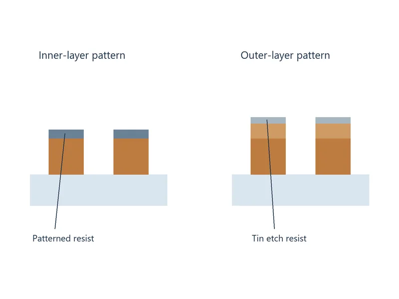
Inner-layer circuits commonly start as copper-clad cores. A patterned resist protects the required conductors while exposed copper is removed; the resulting pattern can be inspected before lamination.
Outer-layer processing can include copper plating and a different etch-resist sequence. We review the starting foil, required finished copper and layer structure rather than assuming every layer follows the same route.
Review Line Width and Spacing with Copper Thickness
| Requirement | Capability or review focus | Design information |
|---|---|---|
| Standard line / space | 4 / 4 mil (approximately 0.102 / 0.102 mm). | Review the specified copper thickness and layer construction with the complete pattern. |
| Advanced line / space | 2 / 2 mil (approximately 0.051 / 0.051 mm). | Fine-line construction reviewed with the selected copper, imaging and process route. |
| Line width and spacing | Smallest conductor and isolation gap on each layer, including local neck-downs and pad clearances. | Nominal geometry, critical locations and any specified finished limits. |
| Copper thickness | Starting foil, required finished copper and the copper structure at the etching stage. | Layer-by-layer copper requirements with units and thickness basis. |
| Thick-copper patterns | Whether the selected copper thickness allows the required conductor shape and gap. | Copper requirement, available routing space and features that cannot change. |
| Controlled impedance | Conductor geometry together with dielectric construction and the required impedance. | Target, tolerance, reference layers, stack-up and permitted adjustments. |
| Critical pads and copper features | Pad dimensions, fine gaps, thermal spokes and narrow copper connections. | Package requirements, functional features and drawing tolerances. |
Control Sidewall Loss and Finished Conductor Dimensions
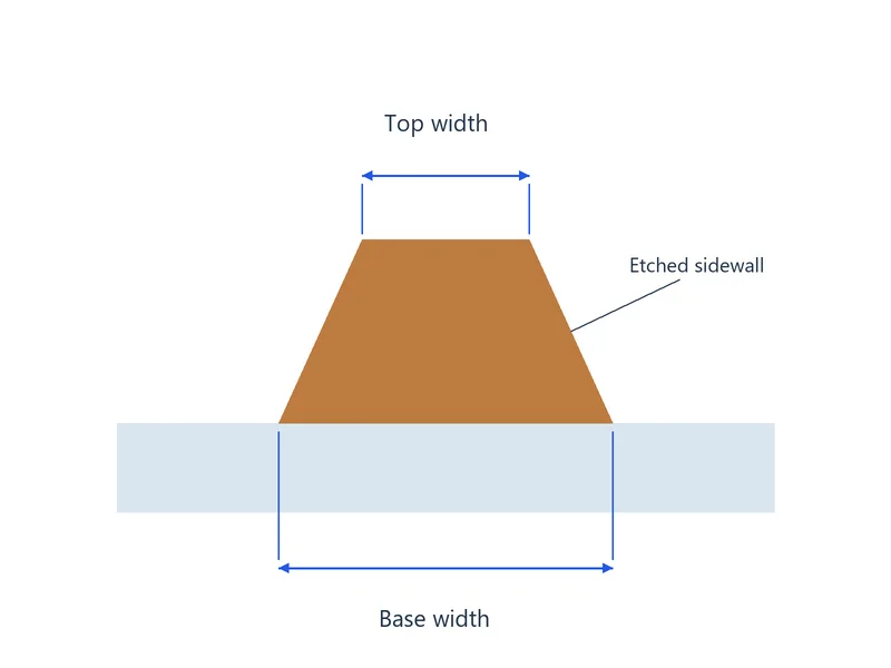
Etching removes copper downward and can also remove material sideways beneath the resist edge. This lateral removal affects conductor width and sidewall shape, so artwork width alone does not describe the finished cross-section.
We prepare process compensation for the selected copper and manufacturing route. Identify the finished-width requirement and measurement basis for critical features so the production data and inspection criteria are consistent.
Preserve the Electrical Purpose of the Copper
Changes to line width, gaps or copper shapes can affect impedance, current paths and component connections. We check proposed changes to critical geometry against the approved design requirements before production.
Small copper islands, thermal spokes and narrow links may have a design function. Identify intentional features and resolve proposed edits rather than removing them solely because they are small.
For thicker conductors, our heavy copper PCB manufacturing service addresses the wider board construction requirements.
Inspect the Pattern Before the Next Manufacturing Step
Optical inspection compares the manufactured copper pattern with the approved reference. We review conductor gaps, residual copper, bridging, notches and narrow features against the specified acceptance requirements.
Electrical testing checks the required connectivity and isolation separately. If a confirmed pattern defect is found, we hold the affected material for the agreed action and verify any authorized correction before release.

Requirements That Help Us Review Your Design
- Layer identity: copper-layer order, orientation and approved data revision.
- Finished geometry: critical line widths, gaps, pads and the measurement basis for inspection.
- Copper requirements: starting and finished thickness where specified, with inner and outer layers identified.
- Electrical priorities: impedance targets, critical current paths and features that must remain unchanged.
- Acceptance and records: applicable requirements, inspection locations and requested measurements or reports.
Files for a PCB Etching Review
- Gerber or ODB++ data with a clear copper-layer map
- Fabrication drawing and approved board revision
- Stack-up, materials and copper thickness for each layer
- Minimum line and gap requirements, plus any local critical dimensions
- Impedance requirements and permitted geometry adjustments
- Quantity, acceptance criteria and required inspection or test records
Submit the released design geometry and identify any compensation already included in the files. We coordinate pattern formation with our PCB fabrication services and the agreed inspection and electrical tests.
PCB Etching FAQs
Send the revised copper thickness and the affected layers for review. Thicker copper can require wider conductors and gaps for the selected process. If the existing geometry is unsuitable, compare routing changes, a different copper distribution or another stack-up while preserving the electrical requirements.
Provide the released nominal design and state whether any compensation is already included. We prepare manufacturing compensation for the selected process. Avoid adding an assumed allowance that could be applied again during CAM preparation; identify critical finished dimensions in the drawing.
Identify the impedance target, tolerance, reference layers and approved stack-up. We review the proposed finished width with copper and dielectric requirements, then obtain the required approval for changes. Define the impedance measurement and report requirements separately from the copper-pattern inspection.
Record the layer, location and board or lot identity, and compare the feature with the approved data and acceptance criteria. Measure a suspect width using the agreed measurement basis. Hold confirmed nonconforming material for review, and verify any authorized correction with the required inspection and electrical checks.
First confirm whether the feature is intentional, such as a thermal spoke, connection, shield or other functional copper. Review the proposed edit against the design requirements and record the approval where required. Do not remove or widen a feature simply to clear a manufacturing warning without checking its purpose.
No. Copper-pattern inspection evaluates the specified physical geometry, while electrical continuity and isolation tests check connectivity. Impedance requires its own agreed measurement. Current capacity and temperature rise depend on the copper cross-section, board construction and operating conditions, which need a separate design assessment or test.
Discuss Your Copper Pattern Requirements
Send your copper-layer files, stack-up and critical dimensions. We will review the etching requirements, proposed manufacturing adjustments and required inspection records with your PCB order.