 Skip to content


Connect the Layers Your Design Needs
We manufacture multilayer PCBs with blind and buried vias for prototypes and production. Our services include stack-up review, via construction, plating, filling where required, inspection and PCB assembly.
Send the layers each via must connect and your proposed stack-up. We review the drilling and lamination sequence before confirming the manufacturing specification and quotation.
Blind, Buried and Through Vias
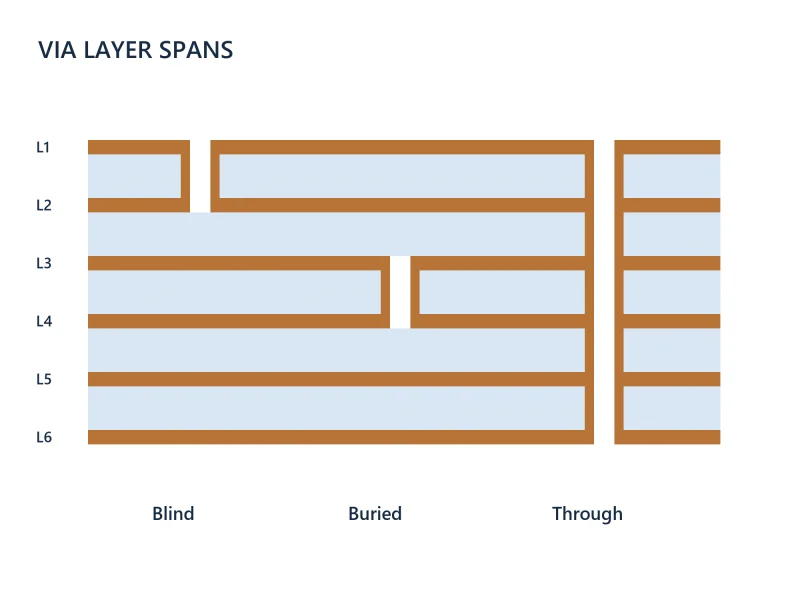
The via type describes which layers the connection reaches in the finished board.
Blind Vias
Connect an outer copper layer to one or more inner layers without extending through the complete board. The permitted span depends on the stack-up and manufacturing route.
Buried Vias
Connect internal copper layers without an opening on either finished surface. These connections are processed within a core or sub-board before the surrounding layers are added.
Through Vias
Extend between the two outer surfaces. They can connect selected layers along the barrel, with clearances on layers that must remain isolated.
Define the Via Spans Before Routing
List the start and end layer of every via group. Review these connections against the core and prepreg arrangement, dielectric thickness and intended build sequence.
A connection such as L1 to L3 needs a construction that can form and plate that span. Depending on the design, the proposal may use a suitable drilled sub-board, a depth-controlled route or a sequence of microvias.
Choose the Manufacturing Route
We select the process from the physical stack-up and required interconnections.
Mechanical Blind Vias
Mechanical drilling can form blind connections through a suitable core or sub-board, or through a controlled-depth process. Hole depth, diameter, plating access and registration must be reviewed together.
Laser Microvias
Laser processing forms small connections in build-up layers. Define the dielectric thickness, target pads, capture pads and any stacked or staggered arrangement before confirming the microvia structure.
Buried Via Processing
Drill and plate the required internal structure while it remains accessible. Complete any specified filling and surface preparation before further lamination.
Match Filling and Capping to the Via Function
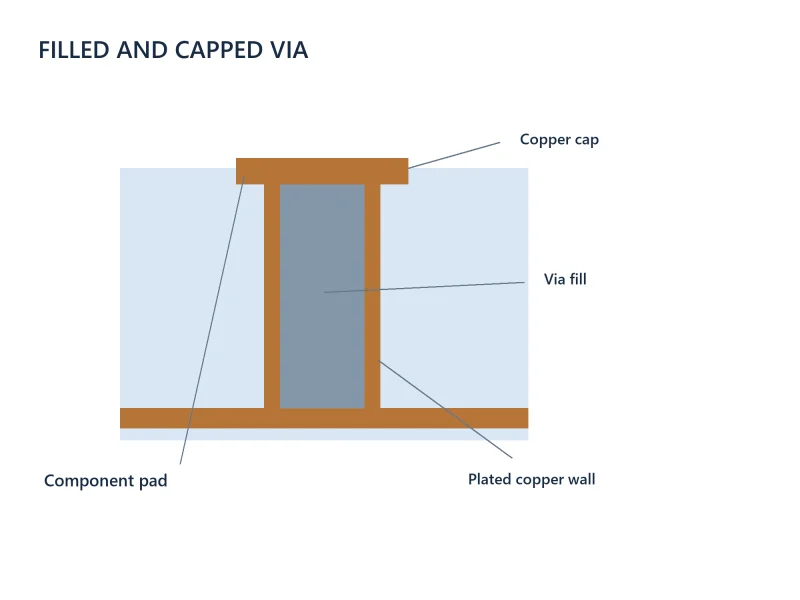
A blind via does not automatically require filling. The specified structure determines whether an open plated hole, copper fill or another filling process is appropriate.
For vias inside solderable component pads, define the filling and pad-surface construction needed for assembly. Stacked microvias also need a suitable filled supporting structure and a controlled connection to the next level. Specify filling, planarization and copper capping separately.
Parameters We Review Together
Provide the required dimensions and tolerances so we can check the complete via construction.
Hole Size and Depth
Specify drilled diameter, finished hole diameter and hole depth separately. State whether an aspect ratio uses hole depth divided by drilled diameter or another agreed definition. A through-hole limit does not define the limit for a blind hole or laser microvia.
Pads and Clearances
Define capture and target pads, annular-ring requirements, drill-to-copper clearance and nearby routing. Registration tolerances must fit the selected structure.
Material and Lamination
Identify core and prepreg materials, finished thickness, copper distribution and the proposed lamination sequence. Review all via groups together rather than approving each span in isolation.
Plating and Filling
Specify hole-wall plating, fill material where required, cap requirements and inspection criteria. Stacked interfaces and via-in-pad surfaces need particular attention.
Choose Stacked or Staggered Connections
Stacked microvias align above one another. Staggered microvias are offset and use an intermediate connection between levels.
Compare the routing area, pad geometry, filling process and reliability requirements for the two arrangements. Use the simplest construction that meets the design, then agree on the manufacturing and acceptance plan.
See our sequential lamination and stacked via services for multi-stage builds.

Inspection for the Specified Via Structure
Agree on inspection and reporting requirements before fabrication.
Connectivity and Registration
Electrical testing checks the required connections and isolation. Registration and dimensional checks address alignment with the approved layer and hole data.
Plating and Microsections
Specify microsections and plating measurements where required to evaluate the relevant via structures. Agree on locations, sampling and acceptance criteria.
Filled and Stacked Structures
Define acceptance for fill, cap and interfaces. Where the project requires thermal or other reliability testing, include the method, conditions and limits in the order.
What Drives Cost and Lead Time?
A via span affects more than the drilling operation.
Build Sequence
Additional lamination, drilling and plating stages increase processing. Review whether the same routing goal can be met with fewer distinct via groups or a simpler build-up.
Filling and Geometry
Filling, planarization, capping and tight registration add work. Small holes must be assessed with their depth, pad sizes and material construction.
Quantity and Acceptance
Material availability, order quantity, test coupons and required reports also affect the quotation. We confirm the production schedule after reviewing the files and material supply.
Files for a Blind and Buried Via PCB Quote
Send the available design files and mark any choices that are still open.
- Gerber or ODB++ data, fabrication drawing and netlist if available
- Layer stack-up, materials and finished board thickness
- Via map showing the start and end layer of each hole group
- Separate drill data for each via span, with clear size definitions
- Pad sizes, clearances and applicable tolerances
- Filling, planarization, capping and via-in-pad requirements
- Impedance targets and critical signal requirements
- Quantity, target date, assembly exposure and acceptance reports
Explore our HDI PCB services for the wider high-density manufacturing scope. Submit your files through our contact page for a construction review and quotation.
Blind and Buried Via PCB FAQs
A direct L1-to-L3 blind via can be feasible, but the layer names alone do not establish a manufacturing route. Send the core/prepreg arrangement, dielectric thicknesses, hole size and pad sizes. We will review whether a single blind via can form the span. If a sequence of stacked or staggered microvias is proposed instead, it requires a separate review of the intermediate pads, routing and build-up.
No. Blind describes the connection from an outer layer to an inner layer. Mechanical drilling, processed sub-boards and laser build-up are different routes. Provide the layer span and geometry so we can select a suitable construction.
Yes, if the revised construction preserves all required connections and can be manufactured. Review the stack-up, pads, clearances, reference paths and manufacturing sequence before changing the via type. Send the existing layout and required layer spans so we can identify any layout changes and revised drill files needed.
If a via opens into a solderable BGA pad, specify how the opening will be filled and finished to provide the required pad surface. An unfilled opening can affect solder volume and joint formation. Send the package details, pad geometry and via structure so we can review the filling and capping requirements.
The construction may add lamination, drilling, plating, filling or inspection stages. Send the complete via map and quantities so the quote reflects the actual sequence. We can compare alternative spans or build-ups where they meet the same routing requirements.
Yes. Send the proposed stack-up, component pitch or fan-out constraints, required layer connections and target board thickness. Identify any fixed dimensions. We can review the proposed via map and manufacturing constraints before you finish the routing.
Discuss Your Blind and Buried Via PCB Project
Send your stack-up, via map and available files. We will review the construction and prepare a manufacturing quotation.