 Skip to content


Teflon / PTFE PCB Manufacturing
PTFE laminate fabrication, multilayer bonding and RF board manufacturing support.
Build the RF Circuit with a Material-Specific Process
Topline Circuit manufactures PTFE-based circuit boards for RF and microwave projects, from prototype builds to production. Our services cover double-sided, multilayer and hybrid structures, with engineering review, controlled impedance and assembly support.
PTFE-based circuit boards are often called Teflon PCBs. Specify the actual laminate supplier, grade, reinforcement or filler, thickness and copper so the material and fabrication route match your design.
Choose the Laminate, Not Just the Polymer Name
Reinforcement, fillers and copper change the properties and processing of a PTFE circuit material.
Reinforced PTFE
Glass reinforcement can take different forms, including woven glass and glass microfibers. Specify the exact product and its electrical and mechanical data rather than assuming all reinforced grades behave alike.
Filled PTFE Composites
Fillers can modify dielectric, thermal and dimensional properties. Compare the grade-specific data with the operating band, loss budget, temperature and manufacturing requirements.
PTFE and Other RF Materials
Rogers RT/duroid, selected RO3000 grades and AGC TLY/TLX families provide PTFE-based options. Rogers RO4003C and RO4350B are hydrocarbon ceramic materials, so a brand name alone does not identify the resin system.
Double-Sided PTFE Circuit Boards
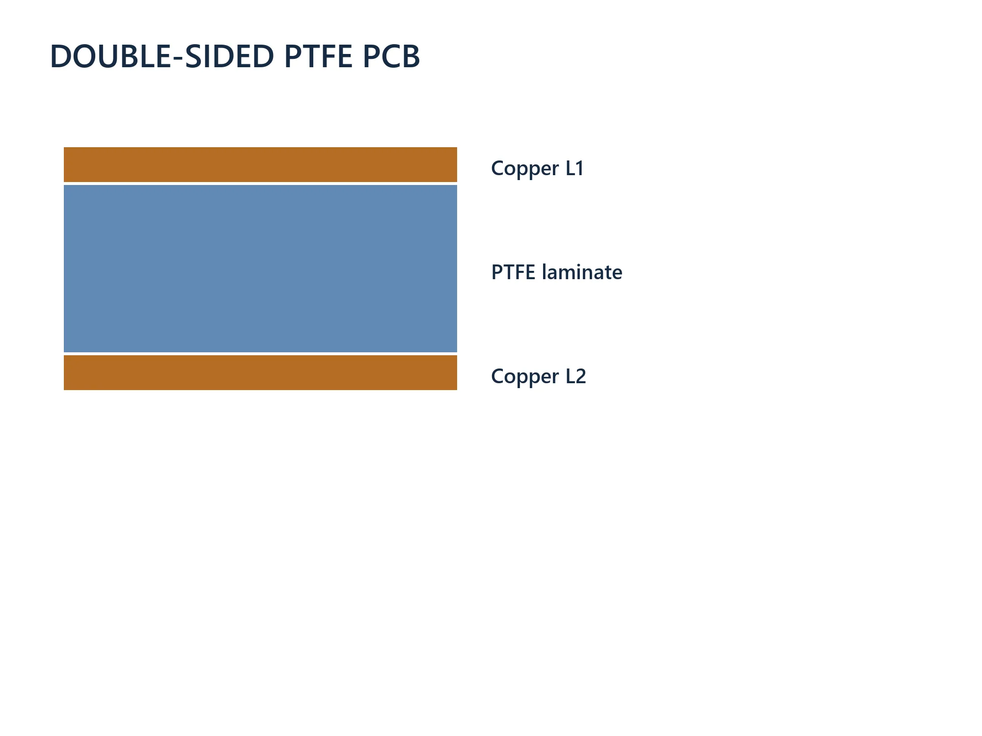
A double-sided construction places copper on both faces of a specified PTFE laminate. Define the circuit and reference functions, core thickness, foil and finished copper.
Review trace geometry, launches, reference continuity and plated connections together. The low dielectric loss of a material does not remove conductor, transition or assembly losses.
Multilayer and Hybrid PTFE Builds
Multilayer constructions require an explicit material schedule between every copper pair. Define the cores, bondply or prepreg and required pressed dielectric spacing.
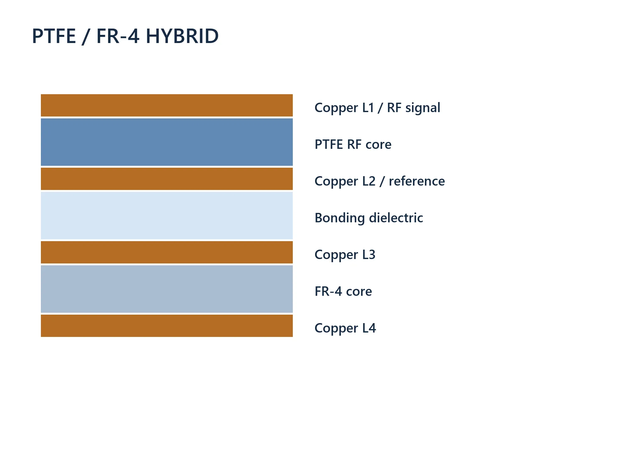
A hybrid can combine a PTFE RF structure with FR-4 elsewhere. Review material compatibility, expansion, registration, bonding and via spans; locate the RF signal and its reference within the intended electrical structure.
Control Handling and Dimensional Stability
PTFE composites need handling and process controls appropriate to their reinforcement and thickness.
Panel Support
Review panel support and handling through imaging, drilling, plating and routing. Limit mechanical damage and unintended deformation of the laminate.
Registration and Geometry
Define layer alignment, critical trace widths, gaps and tolerances. Review process compensation and copper distribution with the actual multilayer construction.
Mechanical Features
Provide the outline, mounting features, slots and finished-thickness requirements. Review routing, edge condition and assembly support for the chosen material.
Prepare the Hole Wall Before Metallization
Drilling exposes a material surface that must support the subsequent metallization process. Select drilling and hole-wall preparation for the exact PTFE composite and interconnect structure.
Review appropriate surface treatment before copper deposition, followed by plating and inspection requirements. A conventional FR-4 desmear route should not be assumed suitable for every PTFE laminate.
Define hole size, span, annular ring and acceptance criteria in the fabrication package. The plated connection and material interface need verification appropriate to the approved build.

Define Bonding and Lamination Before Release
The bonding system is a separate material decision with electrical and manufacturing consequences.
Bond Material
Specify the bondply or prepreg grade and its compatibility with the cores. Include dielectric data and thermal requirements where relevant.
Pressed Spacing and Flow
Define the required finished dielectric spacing and review resin flow with the copper pattern. Supplied sheet thickness alone does not establish the pressed construction.
Sequence and Via Spans
Map conventional, blind, buried or microvia connections to the manufacturing sequence. Review any staged lamination, filling and plated interfaces with the selected materials.
Specify the Electrical Geometry and RF Requirements
The fabricated board must match the material and geometry assumed by the electrical design.
Dielectric Model
Identify the Dk and Df source, test frequency, method and applicable construction. Do not replace model inputs with a generic value for pure PTFE.
Copper, Finish and Mask
State foil or roughness requirements, starting and finished copper, surface finish and mask coverage. Review their effects on loss and RF-sensitive pads or launches.
Impedance and Transitions
Provide targets, tolerances, trace dimensions and reference layers. Identify via transitions, connectors and any change in material or reference geometry.
Agree on Fabrication and Test Acceptance
We support PTFE fabrication and assembly with the acceptance scope defined for each project.
Circuit and Physical Inspection
Specify continuity and isolation requirements, dimensional checks and applicable inspection criteria. Include required records in the production package.
Impedance Verification
Agree on representative coupons, measurement conditions, target values and tolerances when controlled impedance is required.
RF Measurements
Insertion-loss, return-loss or other RF tests need fixtures, frequency ranges, limits and measurement conditions. Agree on the test plan and reporting scope with the quotation.
Assembly Support
For populated boards, review component attachment, thermal processing, panel support and handling. Provide the BOM, placement data and assembly acceptance requirements.
Plan the Quotation Around the Actual Build
Material form, construction and acceptance requirements determine the production proposal.
Material and Quantity
Provide exact grade, thickness, cladding and quantities. Confirm material availability and permitted substitutes for the quoted construction.
Manufacturing Complexity
Layer count, bonding sequence, via structures, mechanical features and panel utilization affect fabrication cost.
Schedule and Documentation
State the target delivery date, material-document requirements and test reports. Confirm the schedule and approved revision before production.
Files for a PTFE PCB Quotation
Send the available package and identify fixed requirements or material choices still under review.
- Gerber or ODB++ data, drill files and fabrication drawing
- Laminate supplier, exact grade, thickness and foil
- Stack-up, bonding materials and via spans
- Operating band, loss budget and impedance requirements
- Finished geometry, surface finish and mask coverage
- Temperature, mechanical and assembly requirements
- Quantity, delivery target and required inspection records
- For assembly projects: BOM, placement data and assembly drawing
Review our Rogers material options for supplier-specific selection. Our PCB fabrication services cover the wider manufacturing scope.
Teflon / PTFE PCB Manufacturing FAQs
No. Compare the loss budget, electrical geometry, temperature, mechanical requirements and available laminate data. Non-PTFE RF materials can meet the requirements of some designs. Share the operating band, critical paths and acceptance targets so the material can be selected for the complete circuit rather than frequency alone.
Do not assume the FR-4 route can be used unchanged. Review handling, drilling, hole-wall preparation, metallization and bonding for the exact PTFE composite. Provide the material code and interconnect structure so the fabrication process and acceptance checks can be planned before production.
Yes, with a construction designed for that combination. Define the RF signal and reference layers, bonding material, pressed spacing and via spans. Review expansion, registration and lamination compatibility, then approve the complete stack-up before releasing routing dimensions.
Only after checking the new construction. Compare dielectric thickness, modeling Dk, loss data, copper and bonding. Recheck impedance, RF response and via or launch geometry, then approve material and artwork changes where required. Similar nominal Dk alone does not establish a drop-in replacement.
Send the layer map, hole sizes and spans, pad dimensions, core grades and proposed bonding materials. Add required pressed spacing, impedance and acceptance criteria. We review drilling, preparation, plating and lamination together so the interconnects fit the selected material construction.
Yes. Send the operating band, impedance and loss targets, available layout, layer count, thickness constraints, temperature range and quantities. Mark fixed requirements and open choices. We can review candidate materials for quotation, then confirm the approved grade, bonding system and production files before manufacture.
Discuss Your PTFE PCB Project
Send your laminate requirement, RF targets and design files. We will review the PTFE construction, fabrication requirements and quotation with your team.