 Skip to content


Flex PCB Stack-Up
Plan flexible layers, bend regions and connector thickness for your circuit.
Build the Stack-Up Around Fit and Motion
We manufacture single-sided, double-sided and multilayer flexible PCBs for prototypes and production. Our flex PCB stack-up support covers polyimide laminates, adhesive and adhesiveless constructions, copper selection, coverlay, local stiffeners and controlled impedance.
Start with how the circuit fits and moves in the product. We review the bending region, connector contact area and component support separately, then define the materials and finished thickness for each region.
Single-Sided Flex: Keep the Bend Region Simple
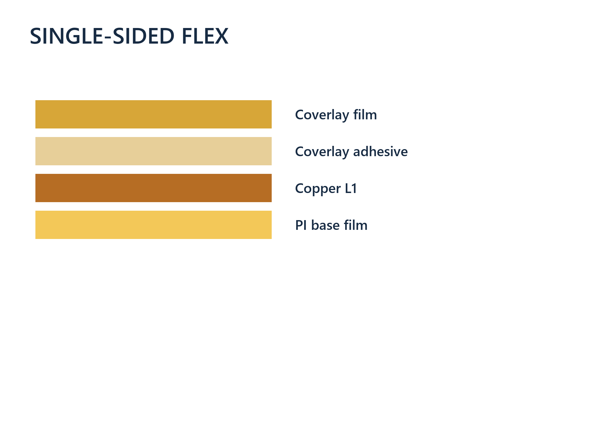
A single-sided flex circuit has one patterned copper layer on a flexible base. The example shows an adhesiveless copper-clad polyimide base with coverlay film and adhesive protecting the circuit side.
One copper layer can reduce the material in the bend region when the routing and electrical requirements permit. Specify exposed contacts, coverlay openings and any access needed from the opposite side.
Define the copper type and finished thickness together with the installed bend geometry. Local stiffeners belong in a separate regional section.

Double-Sided Flex: Connect Both Copper Layers
A double-sided flex circuit places copper on both sides of the base film, with plated connections where the design requires them. Coverlay and openings are defined independently for each side.
The example uses an adhesiveless base laminate, but coverlay adhesive is still present. Include the final plated copper requirement when checking the total thickness.
Review the location of vias, pads and copper transitions relative to the bend region. Two copper layers do not, by themselves, establish suitability for repeated motion.
Connector Support: Define a Separate Local Stack-Up
The connector tail may require a different thickness from the flexible span. Identify the contact side, exposed copper, surface finish, rear stiffener and attachment adhesive on the drawing.
Use the connector manufacturer’s mating-thickness range and tolerance. Measure the complete local construction, including the contact finish and stiffener bondline where present.
A stiffener provides local mechanical support without adding a routing layer. Locate the stiffener edge and coverlay transition outside the intended bend region, and review the transition geometry with the installed shape.

Select Materials by Their Role
Identify each physical constituent rather than combining all insulating layers into one thickness.
Base Laminate
Specify polyimide grade, base-film thickness and adhesive or adhesiveless construction. An adhesiveless base has no separate copper-to-base adhesive layer; other bondlines can remain in the finished circuit.
Copper Foil
Choose rolled-annealed (RA) or electrodeposited (ED) copper for the electrical and mechanical requirements. Distinguish starting foil from finished copper after plating.
Coverlay and Bonding
State coverlay film and adhesive separately, with openings and regional extent. Multilayer flex also needs the interlayer bonding material and finished dielectric spacing defined.
Local Support and Shielding
Specify stiffener material, attachment method and outline. Include shielding film or other local additions in the thickness and electrical review when required.
Choose the Construction for the Bend Duty
An installation fold and a moving interconnect need different design inputs.
Flex to Install
Show the installed radius, bend angle, direction and space envelope. Include assembly handling and any additional bending during installation or service.
Repeated Motion
Provide the motion path, minimum radius throughout travel, expected cycles, speed and operating environment. Review the copper, layer arrangement and validation plan for that duty.
Bend-Zone Layout
Identify bend axes and keep stiffener edges, component joints and plated features out of the intended bending span where practicable. Review trace direction and copper transitions with the mechanical design.
Define Thickness Where It Matters
Use named regions and measurement locations so a compliant flex span does not hide an incorrect connector tail.
Flexible Span
Include base film, copper, coverlay and all relevant adhesives. State the finished thickness and tolerance for the measured region, including whether copper is present there.
Exposed Contacts
Identify where coverlay stops and which face mates with the connector. Include the specified contact finish, backing material and attachment adhesive in the local thickness.
Supported Component Areas
Define stiffener thickness, side, outline and bondline. Review assembly support, flatness needs and the transition into the unsupported flex.
Finished Acceptance
Nominal sheet thicknesses are a starting point. Agree on the finished thickness, tolerance and inspection method for each region based on the manufacturing construction.
When to Use Multilayer Flex
Additional copper layers can provide routing and reference options, with a thicker bonded construction to review.
Routing and Interconnections
Specify the conductive layer count, layer mapping and required via connections. Identify any regions with different layer constructions.
Bonded and Unbonded Regions
Show whether layers remain bonded through each region. An intentionally unbonded construction requires its own fabrication and mechanical review.
Mechanical Tradeoffs
Compare routing needs with the finished thickness and bending duty. Do not carry the bend assumptions of a single-sided circuit into a multilayer construction.
Review Impedance with the Complete Flex Section
Electrical geometry and mechanical flexibility need to work together.
Signal References
Define the signal layer, reference copper and dielectric spacing. Include coverlay and adhesive properties where they affect the structure.
Copper Coverage
Compare solid, patterned or hatched reference copper against impedance, shielding and bending requirements. A change in reference pattern needs an electrical review.
Targets and Testing
Provide single-ended or differential targets, tolerances, trace widths and pair spacing. Agree on impedance coupons, electrical testing and required reports.
Flex PCB Manufacturing Support
We support stack-up engineering and fabrication from prototypes to repeat production.
Construction Options
Single-sided, double-sided and multilayer flex, adhesive and adhesiveless laminates, local stiffeners and coverlay options.
Engineering and Assembly
Material and regional thickness review, controlled impedance, fabrication checks and PCB assembly support for component-bearing flex designs.
Production Release
Approve the stack-up, copper and coverlay data, drill files, stiffener outlines, finish and inspection requirements under a consistent revision.
Files for a Flex Stack-Up Review
Send the available design files and identify dimensions or materials that must stay fixed.
- Gerber or ODB++ data, layer map and drill files
- Flat outline and installed drawing or 3D model
- Bend locations, radius, angle and installation or motion duty
- Connector part number, contact side and mating-thickness requirements
- Materials, copper, coverlay, stiffener and regional thickness requirements
- Impedance targets, quantity and testing requirements
- For assembly projects: BOM, placement data and assembly drawing
See our PCB fabrication services for the wider manufacturing scope. Submit your drawing through our project enquiry page for a flex stack-up review.
Flex PCB Stack-Up FAQs
Use the connector part number and mating drawing to define the contact side, required insertion thickness and tolerance. Include every material present in the insertion region: copper, contact finish, base film, any remaining coverlay and adhesive, and the stiffener and its bondline where used. Send the connector drawing and proposed section so we can review the finished tail thickness before production.
Review the region that is too thick first. Possible changes include the base-film thickness, copper, adhesive system, layer count or local support. Check current capacity, impedance, handling and bending requirements before selecting a thinner construction. A connector region may need a different change from the flexible span.
An adhesiveless base laminate has no separate adhesive layer between its copper and base dielectric. Coverlay adhesive, multilayer bonding material and stiffener attachment adhesive may still be present. List those constituents separately so none is omitted from the thickness or material requirements.
Only after checking the intended motion duty. Send the bend radius throughout travel, angle, direction, expected cycles and environment. Review copper type, thickness, conductor layout and bonded construction, then agree on the validation criteria. A stack-up used for an installation fold is not automatically suitable for repeated motion.
A stiffener can meet a need for local mechanical support when additional routing layers are not required there. If the design needs electrically active rigid layers and their interconnections, compare an integrated rigid-flex construction. Send the component layout, connector needs and mechanical drawing so both options can be assessed.
Yes. Send the outline, available circuit files, installed geometry, connector information, bending duty, electrical targets and quantity. Mark fixed requirements and choices that remain open. We can review a proposed construction for quotation, then confirm the approved stack-up before production release.
Discuss Your Flex PCB Stack-Up
Send your flex design, installed geometry and connector requirements. We will review the material construction, regional thickness and manufacturing quotation with your team.