 Skip to content


8-Layer PCB Stack-Up
Plan signal references, power domains and via connections for your eight-layer PCB.
Allocate Layers Around Your Circuit Requirements
We manufacture eight-layer PCBs for prototype and production orders, with FR-4, high-Tg and RF material options, custom thicknesses, copper weights and controlled impedance. Our engineering team supports stack-up selection, via planning and manufacturing review.
Eight layers give you more options for separating signal groups, reference planes and power domains. Start with the routing and power requirements, then confirm the dielectric spacing and interconnect structure for the actual board.
Four Signal Layers with Three Ground Planes
Signal / Ground / Signal / Power / Ground / Signal / Ground / Signal provides four signal layers, three ground planes and one dedicated power layer. Both outer routing layers have an adjacent ground plane.
For L3, review the distances to L2 ground and L4 power. L6 sits between L5 and L7 ground, while the L4-to-L5 spacing affects the power-ground plane pair.
Plan the power-rail areas without interrupting critical signal references. The actual spacing, plane geometry and return connections determine how the structure performs.


Four Signal Layers with Two Power Planes
Signal / Ground / Signal / Power / Power / Signal / Ground / Signal provides four signal layers, two ground planes and two power layers. It gives you more internal space for power-rail distribution.
Review the L3 and L6 routes against their nearby ground and power planes. Check power-plane partitions, reference continuity and the return path at each layer transition.
The central L4 and L5 layers are both power layers, not a power-ground pair. Assess the power-distribution network and decoupling using the complete plane arrangement.
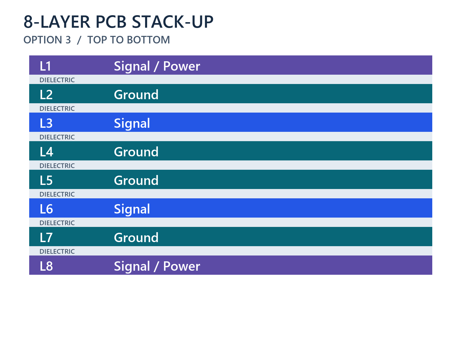
Four Routing Layers with Four Ground Planes
Signal and Power / Ground / Signal / Ground / Ground / Signal / Ground / Signal and Power provides four routing layers and four ground planes. Power uses separate traces or copper areas on the routing layers.
The inner signal layers sit between ground planes. Review the dielectric spacing, route geometry and connections between the ground references, including the transitions to the outer layers.
Reserve enough routing space and copper area for power delivery. Additional ground layers support more reference options, but they do not replace signal-integrity or power-integrity review.
Define the References for Each Signal Group
Assign interfaces to layers based on continuous reference paths and the geometry available in the build.
Internal References
Identify the planes above and below each critical route and the distance to each plane. Check the effect of power-plane splits, voids and via clearances along the route.
Layer and Reference Changes
Plan the return path at each layer transition. Include suitable ground connections when switching ground references and review the required connection when the reference changes between power and ground.
Signal Separation
Separate sensitive and fast-switching routes as required by the interface design. Review spacing, overlap and parallel route lengths rather than relying only on different layer numbers.
Plan BGA Escape and Via Structures Together
The package geometry and route requirements determine the interconnect approach. Eight layers alone do not require HDI or back-drilling.
BGA Escape
Provide the package part number, pitch, land pattern and available routing channels. Review whether through-hole vias can support the escape or whether blind, buried or microvia connections are needed.
Via Spans and Stubs
Identify the layers each critical connection uses and any unused via-barrel sections. Review their electrical effect with the interface requirements before specifying stub control or back-drilling.
Manufacturing Sequence
Define hole sizes, layer spans, filling and other via requirements. We support conventional and specified HDI builds, with the manufacturing sequence selected for the approved structure.
Specify the Physical Eight-Layer Build
The functional layer order defines the copper-layer roles. The material structure defines how the board is manufactured.
Seven Dielectric Regions
Define the pressed spacing between all eight copper layers and confirm the finished board thickness and tolerance. Identify the core and prepreg construction rather than assuming equal spacing.
Material and Copper Data
State material grades and inner and outer copper requirements, distinguishing starting foil from finished copper. Include dielectric constant (Dk) and dissipation factor (Df) requirements with the relevant data source, frequency and test method.
Controlled Impedance
Provide targets, tolerances, signal layers, reference planes and proposed trace and pair geometry. Review these with copper thickness, dielectric spacing and relevant solder-mask effects.
Inspection and Acceptance
Agree on the stack-up revision, permitted substitutions, impedance coupons, electrical testing and required reports. Keep the fabrication drawing and drill information consistent with the approved structure.
Eight-Layer PCB Manufacturing Capabilities
We supply standard and custom eight-layer constructions from prototypes to repeat production.
Materials and Board Thickness
FR-4, high-Tg and RF laminate options are available, with standard and custom finished thicknesses and copper weights selected for the project.
Impedance-Controlled Manufacturing
We support single-ended and differential structures, engineering review, impedance coupons and testing as specified.
Interconnect and Fabrication Options
Our services include conventional multilayer, specified HDI and via treatments, with surface finish and fabrication inspection options for the design.
Prototype to Production
We support prototype, small-batch and production orders. Include the order quantity, required delivery date and inspection criteria for the quotation.
Decide What Eight Layers Need to Solve
Use the extra layers to address an identified routing, reference or power-distribution constraint.
Moving from Six Layers
Mark the congested routes, interrupted references or power areas that do not fit on six layers. Assign each added layer a clear function before comparing constructions.
Staying Within Eight Layers
Check that BGA escape, signal references and power delivery can all be met without creating new plane conflicts. Review the complete geometry and via plan with the material structure.
Considering Ten Layers
Compare ten layers when eight still cannot provide the required routing, reference continuity or power allocation. Assess the revised manufacturing and test requirements along with the electrical design.
Files for an Eight-Layer Stack-Up Review
Send the available design files and identify the decisions that still need review.
- Proposed L1 to L8 functions and fabrication data
- Board outline, finished thickness and tolerance
- Material grades, copper requirements and substitution restrictions
- Interface details, impedance targets and critical route geometry
- BGA land patterns, drill data and via layer spans
- Power rails, current requirements and reference-plane allocation
- Quantity, delivery target and required tests or reports
See our PCB fabrication services for the manufacturing scope. Our sequential lamination and stacked-via services support designs requiring staged build-up.
8-Layer PCB Stack-Up FAQs
Eight layers help when the added layers resolve a specific routing, reference-plane or power-distribution constraint. Mark the blocked routes and plane conflicts in the six-layer layout, then assign a purpose to each added layer. Send both plans with the critical interfaces and thickness requirements. We can review the manufacturing options before your team commits to rerouting.
Not necessarily. Several rails can occupy separate areas of one power layer if the current, copper area and reference requirements can all be met. Map the rails and check where plane partitions sit beneath critical routes. Send that map with the layout so we can compare one- and two-power-layer builds with your design team.
Use the interface requirements and actual plane geometry to decide. Ground is generally preferred, while a continuous power plane can also provide a reference when the return path is properly designed. Identify both neighboring planes, their distances, splits and transitions. Send the critical routes so the selected reference and geometry can be reviewed together.
Not necessarily. Blind or microvias may be needed for BGA escape, while back-drilling addresses unused via-barrel sections that affect signal performance. Provide the BGA part number, pitch, land pattern and critical via connections. Review escape routing and stub effects separately, then select the hole structure and any stub control required by the design.
You can keep the layout if the proposed manufacturing build meets its electrical and mechanical requirements without changing the routing. Send the existing stack-up, material data, impedance table and trace geometry so we can compare the constructions. If the new build changes impedance, reference relationships or via requirements, review the affected geometry and approve the revised production files before release.
Compare ten layers when the eight-layer plan still cannot meet routing, power and continuous-reference requirements together. Identify the unresolved routes or planes and assign a purpose to the added layers. Review the electrical solution, via structure, material build and quotation for both options before selecting the production construction.
Discuss Your 8-Layer PCB Stack-Up
Share your eight-layer design, power domains and critical interfaces. We will review the stack-up, via structure and manufacturing quotation with your team.