 Skip to content


OSP PCB Finish
A flat surface finish that protects copper before PCB assembly.
OSP Finish for Your PCB Production
We provide OSP-finished PCBs for prototype and production orders. Organic solderability preservative forms a thin protective coating directly on exposed copper, helping prevent oxidation before soldering.
OSP preserves the flat profile of the copper pads without adding a metallic finish layer. Send your fabrication files and assembly plan so we can review the finish, packaging and inspection requirements together.
When OSP Fits Your Board
Select OSP based on the pad layout and the process from fabrication to final soldering.
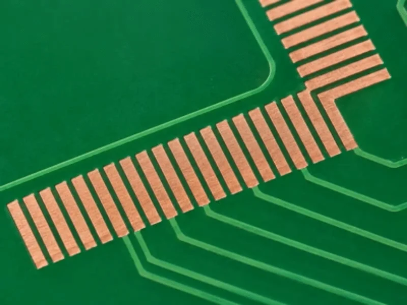
Fine-Pitch Solder Lands
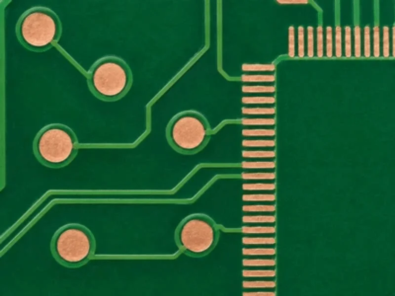
A thin organic coating preserves pad planarity for solder-paste printing. Pad geometry, via treatment and stencil design still need to suit the component package.
Planned Assembly Runs
OSP suits projects with controlled packaging, handling and assembly timing. Include storage and any delay between soldering operations in the production plan.
Lead-Free Soldering
High-temperature OSP systems can support qualified lead-free assembly routes. The selected chemistry and complete thermal history determine the suitable process window.
Plan the Complete Soldering Sequence
Double-sided reflow and later wave or selective soldering expose the finish to several heating operations. Review the first-side profile, interval between operations and the condition needed at the final soldering stage.
Provide the solder alloy, flux, planned reflow passes and any cleaning or rework steps. We review these requirements alongside your PCB assembly process before confirming the finish specification.
Do not select a universal reflow limit from the finish name alone. Use the process window qualified for the selected OSP system and board.
Specify More Than the Finish Name
The drawing and order should define how the OSP coating will be accepted.
Coating Requirements
State OSP as the finish and identify any required chemistry characteristics or coating-thickness limits, with units. Confirm the selected process before fixing those limits.
Standard and Revision
If IPC-4555 is required, identify the applicable revision and customer requirements. Confirm the acceptance basis with the fabrication order.
Measurement and Sampling
Agree on a measurement method suitable for the organic film, the test locations and the sampling plan. Metallic-coating XRF measurement is not a default method for an OSP film.
Solderability and Records
Specify any solderability testing, conditioning, acceptance criteria and reports. Coating thickness and visual appearance alone do not establish solderability after storage or heating.
Protect the Surface Before Assembly
Storage instructions need to match the supplied coating system and packaging.
Keep Packaging Sealed
Keep boards in the supplied protective packaging until needed. Follow the supplier instructions for storage conditions and the permitted storage period.
Control Opened Boards
Record the opening date and assembly history. Avoid touching exposed copper pads and protect opened boards from contamination and unnecessary handling.
Review Delayed or Exposed Lots
Separate boards that have exceeded their specified storage period, have damaged packaging or may have been exposed to moisture. Ask for an assessment before baking, cleaning or putting the boards into assembly.
Review Test Points and Other Exposed Pads
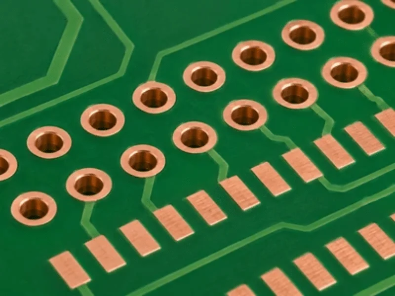
Identify in-circuit test (ICT) points, press-fit holes, wire-bond pads and sliding contacts separately from solder lands. Each interface needs its own contact or assembly requirements.
For ICT, confirm reliable electrical contact with the actual probe system and OSP condition. For press-fit parts, provide the connector specification and hole requirements so finish compatibility can be reviewed.
For wire bonding or repeated sliding contact, specify a finish qualified for that interface. Mark any areas requiring a different finish before releasing the board files.
Compare OSP with Other Finishes
Select the finish for the soldering route, storage plan and exposed-pad functions.
OSP
A thin organic film protects copper without a deposited metal layer. Review handling, storage, thermal exposure and test-point contact.
HASL
A solder coating protects exposed copper. Review the alloy and variation in pad height, particularly where paste deposits and component pitch are small.
ENIG
A nickel-and-gold coating provides a flat metallic surface. Review coating requirements and interface compatibility rather than treating it as an automatic substitute for OSP.
Files for an OSP PCB Quote
Send the current files and identify any finish requirements that remain undecided.
- Gerber or ODB++ files, drill data and fabrication drawing
- Board dimensions, layer count, material and finished thickness
- OSP specification, standard revision and required inspection reports
- Solder alloy, flux, reflow sequence and later soldering or rework steps
- Expected storage period, packaging and assembly timing
- Test points, press-fit holes and any non-solder contact areas
- Order quantity and delivery requirements
Explore our PCB fabrication services and lead-free PCB options for related manufacturing requirements.
OSP PCB Finish FAQs
Do not release the lot based on appearance alone. Keep it separate and provide the fabrication date, packaging condition, opening date and storage history. The board supplier and assembly team can assess whether solderability verification or an approved reprocessing route is needed before use.
Yes, when the selected OSP system and complete assembly route are qualified for those exposures. Share the profiles, number of heating operations, intervals, solder alloy and flux. Confirm the surface condition needed at the final soldering stage before approving production.
Compare the affected pads with the first-side thermal profile, time between operations, storage and handling records, and flux condition. Check for contamination and whether the planned process stayed within its qualified window. Share pad photographs and profile data before changing the temperature or flux settings.
Ask the board supplier and assembly team to approve a procedure for the actual material and finish. Uncontrolled baking or cleaning can affect the protective film and solderability. Provide the exposure history and board construction so the need for drying, verification or reprocessing can be assessed.
Identify the test pads and validate contact with the intended probe type, fixture and board condition. Review contamination, probe maintenance and the contact requirements together. If reliable contact cannot be established, agree on a test-pad or finish change before production.
Send the fabrication files, quantity and known assembly route. Include storage expectations, any IPC-4555 revision requirement, inspection reports and non-solder pad functions. Mark undecided items so we can review them for quotation and agree on the final specification before manufacturing.
Discuss Your OSP PCB Requirements
Share your board files and assembly plan. We will review the OSP finish, packaging and inspection requirements with your team.