 Skip to content


PCB Testing & Inspection Services
Inspection and Testing for Bare Boards and Assemblies
We provide inspection and testing for bare PCBs and assembled boards, from fabrication checks to electrical and functional verification. Available methods include SPI, AOI, X-ray, flying probe, in-circuit testing (ICT) and functional testing.
Share your board files, component packages and acceptance requirements. We help define the methods, coverage and records needed for your project before production.

Inspection and Test Methods
Optical inspection, X-ray and electrical tests answer different questions. We combine the required methods to cover visible assembly features, hidden joints and specified electrical behavior.
Solder Paste Inspection (SPI)
Check solder-paste deposits after stencil printing and before component placement. With 3D SPI, measure deposit position, height, area and volume against the programmed limits.
Automated Optical Inspection (AOI)
Check visible component placement, markings and accessible solder joints. Identify missing or shifted components, visible polarity errors and solder defects using the programmed criteria.
X-Ray Inspection
Examine hidden solder joints beneath BGA, QFN and other bottom-terminated packages. Review joint geometry, bridging and voiding against the agreed inspection criteria.
Flying Probe Testing
Use moving probes to check accessible electrical nets and selected circuit characteristics. Use the appropriate test system for bare-board continuity and isolation checks or populated-board measurements. Coverage depends on probe access and circuit design.
In-Circuit Testing (ICT)
Use a dedicated fixture and test program to check accessible connections and selected component values. Coverage depends on test-point access, circuit topology and the fixture design.
Functional Testing
Power the assembly and verify the functions defined in the approved procedure. Tests can include supply behavior, interfaces, outputs and operation under specified loads.
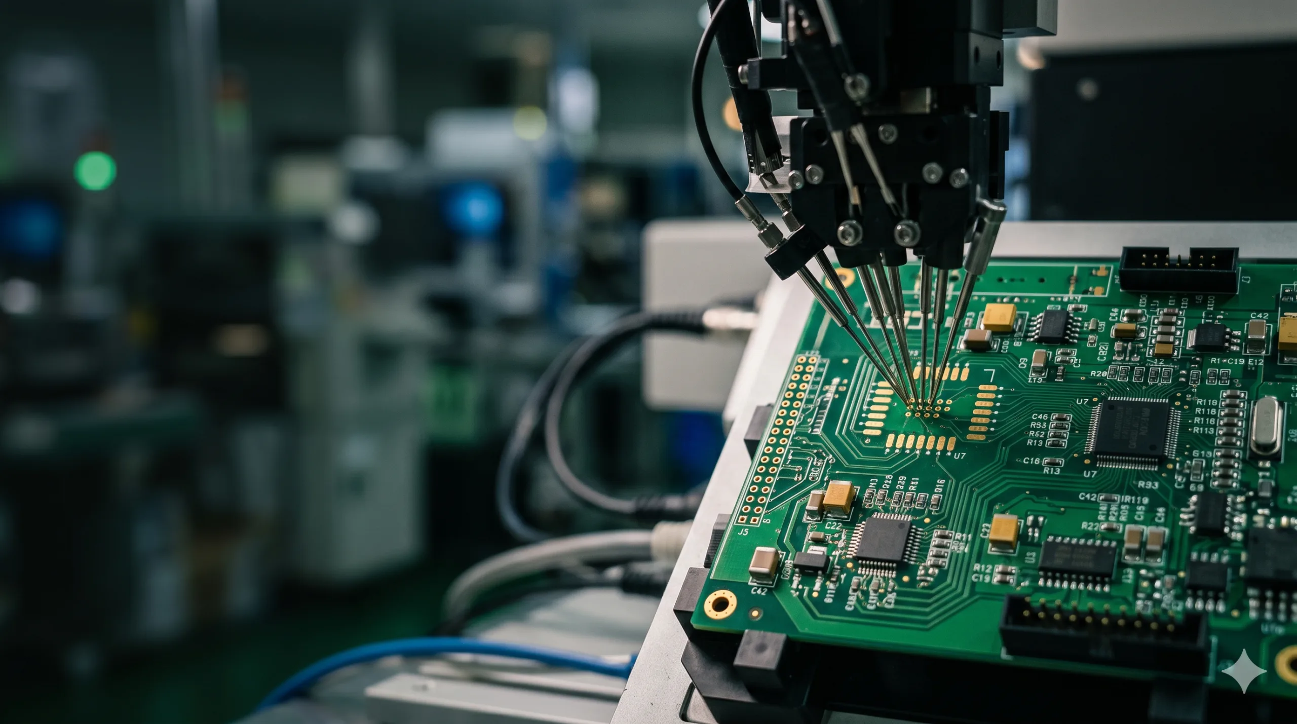
Bare PCB Inspection and Electrical Tests
For bare PCB fabrication, inspection focuses on the board structure and manufacturing data before components are fitted.
- Visual and dimensional checks of the board outline, holes and surface features
- AOI of inner-layer copper patterns before lamination
- Electrical continuity and isolation tests for opens and shorts
- Controlled-impedance measurements against specified targets and tolerances
- Microsection inspection of plating, vias and layer construction when required
Include the fabrication drawing and any required impedance or inspection reports with your enquiry.
Assembly Inspection Through Final Verification
For PCB assembly, we combine process inspection with the required electrical and functional tests. Inspection points can include solder-paste printing, post-reflow assembly and final release.
Fine-pitch components, hidden solder joints and dense layouts need different coverage. BGA and QFN joints can be examined by X-ray; ICT and functional tests address selected electrical faults and operating requirements.
Programming, test fixtures and customer-supplied equipment are included in planning when needed for the agreed test procedure.
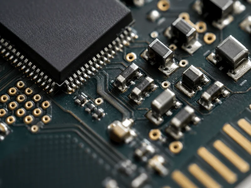
Plan Coverage Around Your Board
Tell us which faults matter most and which results you need to verify. This helps us choose the inspection stage, test access and equipment needed for the build.
Missing Parts or Wrong Orientation
Use AOI and visual inspection against the approved BOM, placement data and assembly drawing. Confirm polarity markings and component identification before inspection programming.
Hidden Solder Joint Concerns
Use X-ray for packages whose joints cannot be viewed directly. Define the packages to inspect, image requirements and acceptance criteria before production.
Opens, Shorts or Incorrect Values
Select bare-board electrical tests, assembly flying probe or ICT according to the build stage and accessible circuit nodes. Define the required fault coverage with the test plan.
Power-Up and Operating Behavior
Use functional testing with defined supply settings, loads, firmware, interfaces and pass/fail limits. Record the specified results for each required operating condition.
What to Send for a Test Plan
Send the current project revision and tell us whether the order is for bare boards, assembly or both.
- Gerber or ODB++ data, fabrication drawing and stack-up
- BOM, placement data and assembly drawings for populated boards
- Schematic, netlist and test-point information for electrical test planning
- Required inspection standard and revision, applicable class and customer-specific acceptance criteria
- Test limits: continuity resistance, isolation resistance and test voltage for bare boards; specified impedance targets and tolerances; operating voltage, loads and pass/fail limits for functional tests
- Firmware, programming instructions and fixture or interface details
- Required reports, traceability fields and any sampling instructions
We review the supplied information and identify the remaining requirements before confirming the test scope.
Testing and Inspection FAQs
Send your board files, component packages and acceptance requirements. Bare boards need a different test plan from populated assemblies. For assemblies, we review visible and hidden joints, electrical access and required functions. For bare boards, we review connectivity, construction and specified measurements before proposing the test coverage.
No. AOI checks visible features and cannot directly view joints hidden beneath the package. X-ray can examine those joints for features such as bridging and voiding. Electrical and functional tests can provide additional coverage for the specified circuit connections and functions.
Flying probe uses moving probes and can avoid a dedicated bed-of-nails fixture. ICT uses a dedicated fixture and program, which can suit repeat production. Send the schematic, test-point layout and quantity so we can review access, coverage and setup requirements.
Provide a test procedure with the functions to check and pass/fail limits. Include supply settings, loads, signal connections, firmware and any required fixtures or reference units. If the procedure is incomplete, tell us the operating behavior you need verified so we can discuss the missing details.
Yes. Specify the records needed before the order is released, such as X-ray images, electrical test results, impedance measurements or functional test logs. Include the required format, board identification and acceptance limits so these can be included in the agreed scope.
We identify the failed item and review it against the approved criteria. The next action may involve clarification, rework or replacement, depending on the cause and agreed requirements. Reworked boards are checked again using the applicable inspection and test steps before release.
Discuss Your Inspection and Test Requirements
Share your board files, acceptance criteria and required reports. We will help define the inspection and test scope for your project.