
With the rapid development of new energy vehicles, industrial automation, energy storage systems, and high-performance communication equipment, modern electronic devices now demand higher stability, integration density, and thermal performance from power control systems. Traditional PCBs are no longer sufficient for applications requiring high power density, compact structures, and high-speed signal transmission. As a result, HDI TR power control board PCBs have become a key component in advanced electronic products. HDI (High Density Interconnect) technology enables more complex functions within limited space through higher routing density, smaller vias, and finer circuit layouts, while also improving signal integrity and overall operational stability.
What Is an HDI TR Power Control Board PCB?
An HDI TR power control board PCB is a power management circuit board designed using high-density interconnect technology, commonly used in power conversion systems, energy management equipment, and industrial control applications. These PCBs improve circuit integration capability and optimize current distribution and thermal performance through microvias, blind and buried vias, and multilayer structures.
Key characteristics include:
- High-density circuit design: Integrates more electronic components within limited board space, making it suitable for complex control systems.
- Optimized power management capability: Improves current transmission efficiency while reducing energy loss.
- Enhanced signal integrity: Shortens signal paths and minimizes electromagnetic interference and transmission delay.
- Support for high-speed and high-power applications: Suitable for industrial equipment, AI systems, and new energy vehicle applications.
- Improved structural stability: Multilayer PCB structures increase reliability and anti-interference performance.
High-power control boards often require wider traces, optimized power layouts, and higher-grade components to ensure long-term stable operation.
Core Process Comparison of HDI TR Power Control Board PCBs
Different manufacturing processes directly affect PCB performance and application scenarios. The table below compares common technologies used in HDI power control boards:
| Process Type | Main Function | Technical Features | Typical Applications |
| Microvia Technology | Increases routing density | Smaller via size and lower space occupation | HDI high-density PCBs |
| Blind/Buried Via Technology | Enhances interlayer connection | Improves routing efficiency | Multilayer control boards |
| Heavy Copper Process | Improves current carrying capability | Supports high-current transmission | Power control systems |
| ENIG Surface Finish | Enhances soldering reliability | Strong oxidation resistance | Industrial and automotive electronics |
| Multilayer Lamination | Improves structural stability | Better anti-interference performance | High-frequency and high-speed devices |
| High-Frequency Materials | Improves signal integrity | Reduces signal loss | Communication and AI equipment |
Fast Prototyping Process for HDI TR Power Control Board PCBs
Fast prototyping is a critical stage for verifying PCB design reliability and identifying potential issues before mass production.
- PCB design review: Optimizes routing layouts and stack-up structures through DFM analysis to improve manufacturability.
- Gerber file verification: Checks routing, hole positions, and pad data to reduce manufacturing errors.
- Material selection: Chooses suitable substrates such as FR4, high-TG materials, or high-frequency laminates based on power requirements.
- Laser drilling and lamination: Completes HDI microvia processing and multilayer structure fabrication.
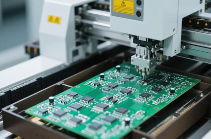
- SMT assembly and soldering: Installs components and performs soldering validation.
- AOI and X-ray inspection: Detects soldering quality and internal structural reliability.
- Functional testing: Simulates real operating conditions to verify PCB performance.
Some advanced HDI PCBs also combine high-frequency materials and hybrid lamination processes to support AI systems, high-speed communication, and industrial control applications.
Advantages of HDI TR Power Control Board PCB Mass Production
HDI power control boards demonstrate significant technical and cost advantages during mass production.
- Improved production consistency: Automated equipment and standardized processes ensure stable batch quality.
- Reduced system size: High-density layouts minimize PCB dimensions and save overall device space.
- Enhanced thermal performance: Optimized copper thickness and stack-up structures improve heat dissipation capability.
- Higher long-term reliability: Suitable for continuous high-load operating environments.
- Support for complex function integration: Enables integration of more control and communication modules.
Advanced HDI structures and high-frequency PCB technologies can significantly improve power conversion efficiency and overall system performance.
Application Areas of HDI TR Power Control Board PCBs
HDI TR power control board PCBs are widely used across various high-end electronic industries.
- New energy vehicles: Used in BMS systems, motor controllers, and onboard power systems.
- Industrial automation: Applied in servo controllers and industrial power equipment.
- AI and communication devices: Supports high-speed data processing and stable power delivery.
- Energy storage systems: Used in battery management and energy conversion modules.
- Medical electronic devices: Meets high reliability and long-term operational requirements.
Complex PCB structures and high-density designs have become a major direction in modern electronic product development.
Future Trends: Integration of High Density, High Power, and Smart Manufacturing
As electronic devices continue evolving toward higher performance and smaller sizes, HDI power control board PCBs are also advancing rapidly. Future manufacturing technologies will focus more on high-precision processing, automated inspection, and intelligent manufacturing management. AI visual inspection systems and MES platforms will provide higher levels of quality control and production traceability. Meanwhile, high-frequency materials, heavy copper technology, and higher-layer HDI structures will continue improving power control system performance, allowing PCBs to play a more important role in new energy vehicles, AI servers, and advanced industrial equipment.
In advanced electronics manufacturing, HDI TR power control board PCBs are no longer just ordinary circuit boards. They have become a critical foundation that determines system performance, operational stability, and long-term reliability. Whether in fast prototyping or mass production stages, high-quality HDI PCBs help companies shorten development cycles, improve product performance, and strengthen market competitiveness. For businesses seeking high-density, high-power, and highly reliable electronic solutions, choosing a mature and stable HDI PCB manufacturing and assembly solution is an essential step toward product advancement and industrial growth.
Manufacturer Warranty and Contact Support
You can send us your dimensions, layer count, impedance requirements, and application scenarios, and we will provide more suitable recommendations based on your actual needs to help you enter mass production faster.If you would like to learn how we can support your project, please contact us for professional advice.
WhatsApp: +86 13425156463
VK: vk.com/id1058761391
Email: sales@toplinecircuit.com
Website: www.toplinecircuit.com
Address: 3rd Floor, Building B3, Yanchuan North Industrial Park, Yanluo Street, Bao’an District, Shenzhen, China


