


")
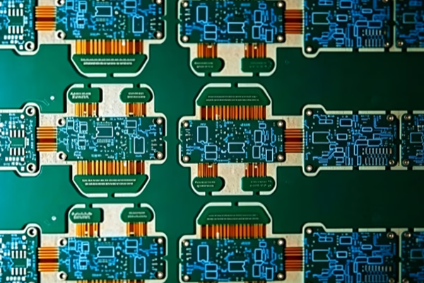
In high-reliability electronic products, a 6-layer rigid-flex PCB is no longer just a “more complex circuit board,” but a key solution that enables compact layouts, stable interconnections, and long-term durability. Especially when the PCB must handle high-speed signal transmission while also enduring plugging/unplugging, friction, bending, vibration, and long-term operation, a conventional structure often cannot meet all requirements at the same time. In this case, a 6-layer rigid-flex PCB with FR4 stiffeners and hard gold plating becomes a more suitable solution for high-reliability connections, high-frequency use, and precision assembly scenarios. It combines rigid-flex architecture for spatial interconnection, FR4 stiffeners for localized mechanical reinforcement, and hard gold surface treatment for improved contact durability and electrical stability, ensuring reliable operation even in complex environments.This type of structure is commonly used in military electronics, handheld medical devices, wearable technologies, RF modules, and industrial control systems. It focuses not only on “whether it can be manufactured,” but more importantly on “whether it can operate reliably over time.”
What Is a 6-Layer Rigid-Flex PCB with FR4 Stiffeners and Hard Gold Plating?
What is a 6-layer rigid-flex structure?
A 6-layer rigid-flex PCB is a type of circuit board that consists of six conductive layers and includes both rigid and flexible areas. The rigid sections are typically used for mounting components such as chips, connectors, and controllers, while the flexible sections are used for spanning spaces, connecting modules, and enabling bending paths. It integrates the structural stability of rigid PCBs with the spatial flexibility of FPCs into a single board, making it ideal for compact, highly integrated, and structurally complex products.
What is the role of FR4 stiffeners?
FR4 stiffeners are typically applied at rigid-to-flex transition areas or at regions requiring higher mechanical support, such as connectors, solder pads, and board edges. Their purpose is not to change circuit functionality but to enhance mechanical strength and reduce stress concentration during bending or repeated insertion/removal cycles. In simple terms, FR4 stiffeners make flexible areas more stable and solder joints more durable, preventing lifting, cracking, or delamination under mechanical stress.
Why hard gold plating matters?
Hard gold, also known as electroplated hard gold, is a surface finish designed for high-wear electrical contact areas. It ensures low contact resistance and excellent wear resistance, making it ideal for edge connectors, gold fingers, and sliding contacts. Unlike ENIG, hard gold can withstand thousands of mating cycles without performance degradation. It is especially suitable for high-reliability connector interfaces where repeated insertion and stable long-term electrical contact are required.
Feature
| Item | Description |
| Structure | 6-layer rigid-flex stack-up for compact complex routing |
| Reinforcement | FR4 stiffeners at rigid-flex transition areas |
| Surface finish | Hard gold plating for durable and corrosion-resistant contacts |
| Standards | IPC Class 2/3 compliant manufacturing |
| Capability | Tight impedance control and fine-pitch routing capability |
| Compliance | RoHS-compliant UL-certified materials |
| Applications | Military electronics, handheld medical devices, wearables, RF modules, industrial control |
How Is This PCB Made?
Requirement definition and structural planning
The first step is not layout design but requirement analysis. Engineers must define rigid areas, flexible areas, bending zones, high-speed signal paths, and mechanical stress points. FR4 stiffeners and hard gold plating must be considered from the early design stage, not added later. Without proper planning, issues such as improper stiffener placement, premature wear of gold fingers, or impedance mismatch may occur.
Stack-up design and routing allocation
The stack-up design ensures stable electrical reference between signal, power, and ground layers. High-speed signals are typically placed close to solid reference planes to reduce reflection and crosstalk. Flexible areas must minimize vias and sharp bends to ensure mechanical reliability. For gold-finished contact areas, plating thickness and uniformity must be carefully controlled to ensure long-term stability.
Manufacturing process flow
| Step | Function |
| Inner layer fabrication | Defines internal circuitry |
| Lamination | Bonds rigid and flexible layers |
| Drilling & via plating | Establishes interlayer connections |
| Outer layer imaging | Defines outer circuits |
| Hard gold plating | Forms wear-resistant contact surfaces |
| FR4 stiffener bonding | Reinforces mechanical structure |
| Electrical testing | Ensures continuity and impedance compliance |
Why manufacturing is more complex?
The challenge is not layer count, but the coexistence of multiple requirements: rigidity, flexibility, wear resistance, impedance control, and mechanical durability. Any weak point in the process can affect overall reliability, which makes process control and engineering experience critical.
How to Optimize a 6-Layer Rigid-Flex PCB?
Function of hard gold surface treatment
Hard gold is especially suitable for high-frequency mating cycles and wear-prone contact areas. Gold fingers, edge connectors, sliding contacts, and test interfaces all require stable electrical performance and wear resistance. Hard gold provides low contact resistance and maintains stable conductivity even after thousands of insertions, making it essential for high-reliability systems.
Impedance control and fine-pitch routing
Impedance control is critical for high-speed and RF applications. Line width, spacing, copper thickness, dielectric properties, and via structure must be tightly controlled to ensure signal integrity. Fine-pitch routing capability allows dense layouts while maintaining manufacturability. Poor control may lead to signal reflection, timing issues, or transmission loss.
FR4 stiffener structural optimization
FR4 stiffeners are not simply “added plates,” but carefully engineered reinforcement structures. Their placement, thickness, and orientation must match mechanical stress distribution. Over-thick stiffeners reduce flexibility, while insufficient reinforcement leads to mechanical failure. Proper design ensures both durability and flexibility balance.
Technical optimization points
| Optimization | Method | Effect |
| Impedance control | Precise line width & dielectric design | Stable high-speed signals |
| Flex design | Reduce vias, avoid sharp bends | Improved flex life |
| Stiffener design | Proper placement and thickness | Enhanced mechanical strength |
| Contact optimization | Uniform hard gold plating | Improved durability |
| Process control | Tight lamination and plating control | Higher consistency |
What Materials Are Used?
Flexible area materials
Flexible areas typically use polyimide (PI) due to its high thermal stability, flexibility, and mechanical durability. PI can withstand bending stress and high-temperature environments, making it ideal for dynamic interconnections. Conductors are usually made of high-ductility copper to improve bending fatigue resistance.
Rigid area materials
Rigid areas commonly use FR4 due to its mechanical strength, dimensional stability, and mature manufacturing process. It provides solid support for components and connectors. In high-performance applications, enhanced laminate materials may be selected for improved electrical performance.
Surface finish and reinforcement materials
Hard gold plating is used for contact areas to ensure wear resistance and long-term electrical stability. FR4 stiffeners are applied at transition and connector areas to enhance structural strength. Together, they improve durability and reliability.
| Material area | Common material | Function |
| Flexible substrate | PI (Polyimide) | Flexibility & thermal resistance |
| Flexible conductor | High-ductility copper | Bending durability |
| Rigid substrate | FR4 | Structural support |
| Surface finish | Hard gold plating | Wear-resistant electrical contact |
| Reinforcement | FR4 stiffener | Mechanical reinforcement |
Frequently Asked Questions
When should this structure be used?
Many customers ask when a 6-layer rigid-flex PCB with FR4 stiffeners and hard gold plating is truly necessary. The answer is: when the product requires both mechanical bending and high-reliability electrical contact. For example, edge connectors that require repeated insertion, gold fingers that must maintain stable conductivity, and internal structures that require both bending and rigid mounting all benefit from this solution. It is also widely used in military systems, medical handheld devices, wearable electronics, and RF modules where durability, compactness, and signal stability are all critical. In short, if your product involves bending + insertion cycles + high-density routing + long-term reliability, this structure is highly recommended.
Why choose Topline Circuit for custom rigid-flex PCB?
Founded in 2000 and headquartered in Shenzhen, China, Topline Circuit is an electronic solution provider offering PCB layout, manufacturing, assembly, testing, and validation services. Our product portfolio includes high-reliability flexible PCBs, rigid-flex PCBs, RF/microwave PCBs, HDI PCBs, and rigid PCBs. As a recognized technology-driven manufacturer, we provide fast turnaround times with fully in-house solutions, offering a true one-stop service experience. Our PCBs are widely trusted in government, medical, instrumentation, aerospace, industrial, and communication sectors.
After-sales service
We specialize in providing high-performance, high-reliability PCB solutions. Whether for consumer electronics, industrial applications, or communication equipment, we can customize the most suitable product according to your requirements. Please contact us via email for quotation and technical consultation.Email: [sales@toplinecircuit.com](mailto:sales@toplinecircuit.com)


")

