


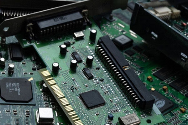
BGA is an advanced integrated circuit packaging and assembly technology. Its core feature is the matrix arrangement of solder balls on the bottom of the chip, used for electrical and mechanical connections to the PCB. Compared to traditional leaded packages, BGA eliminates the need for external pins, utilizing the bottom solder ball array for connections, thus significantly improving connection density and performance. In actual manufacturing, BGA assembly is typically part of SMT (Surface Mount Technology), where solder paste printing, placement, and reflow soldering are used to connect the solder balls to the PCB pads. Due to its larger solder ball spacing and shorter leads, BGA offers significant advantages in high-speed, high-frequency circuits, but also places higher demands on process control.
BGA Packaging Capabilities and High-Density Mounting Support
BGA packaging demonstrates outstanding integration capabilities in electronics manufacturing. Its bottom-mounted ball array enables electrical connections, allowing for more complex circuit designs within a limited space. This structure overcomes the limitations of traditional pin distributions, concentrating more connection points at the bottom of the package, thus effectively improving overall layout efficiency.
In high-density mounting, BGA packaging better meets the demands of refined PCB designs. Its surface array connection optimizes wiring structures, reduces signal path lengths, and improves space utilization, resulting in a more compact board design. For products requiring both high performance and miniaturization, this packaging method enables higher-level functional integration without increasing board area, providing stable support for complex systems.
BGA Assembly Process and Thermal Profile Control
During BGA PCB assembly, thermal profile is one of the key factors affecting soldering quality. Since BGA solder joints are located at the bottom of the package, any temperature unevenness can lead to defects such as cold solder joints, voids, or open circuits. Before production, we conduct rigorous Design for Manufacturability (DFM) analysis to comprehensively evaluate the PCB structure, BGA device parameters, and soldering process, and develop optimized reflow soldering profiles.
Thermal process design primarily considers the following factors:
- BGA size and heat capacity distribution
- PCB layer count and copper foil thickness
- Solder ball material type (lead-containing or lead-free)
- Surface treatment process compatibility (ENIG / HASL / OSP, etc.)
- Thermal stress and warpage control for large-size BGAs
For large-size or high-I/O BGA devices, we optimize the heating profile to distribute heat more evenly across the soldering area, thereby reducing voids and minimizing the risk of solder joint defects.
Comparison of Lead-containing vs. Lead-free BGA processes
| project | Lead-containing BGA process | Lead-free BGA process |
| reflux temperature | Low, wide process window | Higher, with stricter control requirements |
| heat curve | Relatively stable and simple in process | Multi-stage precise temperature control |
| Weld joint risk | Low short-circuit risk | Cold welding risks require focused control |
| Application areas | Traditional electronic products | Environmentally Friendly and High-Reliability Products |
BGA soldering, repair, and ball placement services
For R&D verification, small-batch pilot production, and failure repair needs, we offer complete BGA soldering, rework, and ball-mounting solutions to help customers shorten development cycles, reduce manufacturing risks, and improve overall product yield.
BGA Soldering Services: We provide professional soldering services for PCBs containing a small number of BGAs or fine-pitch devices, particularly suitable for R&D prototyping and engineering verification stages.
- Supports high-density BGA and micro-package device mounting
- Utilizes precision reflow soldering profile control to reduce thermal shock
- Compatible with multilayer HDI PCBs and complex layout designs
- Ensuring soldering consistency and electrical connection reliability
BGA Rework Service: For manufacturing defects, component failures, or design adjustments, we offer standardized BGA rework processes to ensure that circuit boards can be safely repaired and restored to function.
- Safely remove BGA components to avoid damaging PCB pads
- Clean and smooth the pads to restore solderability
- Reprint solder paste or rebuild solder balls
- Precisely align and mount components and perform reflow soldering
- Perform functional testing and quality verification after completion
BGA Ball Repositioning Service: When BGA device solder balls are damaged or need to be reused, we provide professional ball repositioning services to restore the device to a reassembleable state.
- Precise control of solder ball diameter and spacing consistency
- Support for multiple BGA package types (PBGA / CBGA / FCBGA, etc)
- Use of high-precision fixtures to ensure stable solder ball arrangement
- Improved device reusability and reduced overall cost
Rework Process Quality Control: All BGA rework processes are conducted under strict process control to ensure that the reworked PCBs achieve near-original manufacturing reliability.
- Controlling the heating profile to avoid PCB thermal damage and warping
- Preventing pad detachment and secondary oxidation
- Precisely controlling solder volume and wettability
- Recording process parameters throughout the entire process to ensure traceability
Post-repair inspection and verification: Products that have undergone repair and solder ball re-bonding undergo multiple tests to ensure that their electrical and structural performance meets requirements.
- X-ray inspection of solder joint structural integrity
- Inspection of solder ball voids, misalignment, and bridging issues
- Electrical function testing to verify overall performance
- Additional reliability spot checks for critical products
BGA X-ray Inspection and Quality Control
Since BGA solder joints are located at the bottom of the device and cannot be directly observed using traditional optical inspection methods, X-ray inspection becomes a core component of BGA quality control.
- We use high-resolution industrial-grade X-ray inspection equipment to perform non-destructive analysis of the internal structure of solder joints, effectively identifying and quantitatively assessing soldering defects.
- Our inspection capabilities include solder ball void analysis, solder joint bridging detection, cold solder joint and poor solder joint identification, solder ball misalignment assessment, and analysis of PCB internal via structure anomalies (including via-in-pad design and blind/buried via structures).
Through two-dimensional and three-dimensional X-ray imaging technology, we can deeply analyze the internal state of solder joints, achieving higher-precision quality traceability and supporting process optimization.
Summary of BGA Process Advantages
Compared to traditional packaging methods, BGA packaging technology offers significant advantages in high-performance electronic design. It provides higher I/O density, shorter signal paths, and superior electrical performance, while also offering excellent heat dissipation, making it suitable for high-power and high-speed signal applications. Furthermore, the BGA structure is ideally suited for high-density HDI PCB designs, facilitating product miniaturization and performance improvements. In modern communications, computing, and industrial electronics, BGA has become one of the mainstream packaging choices.