


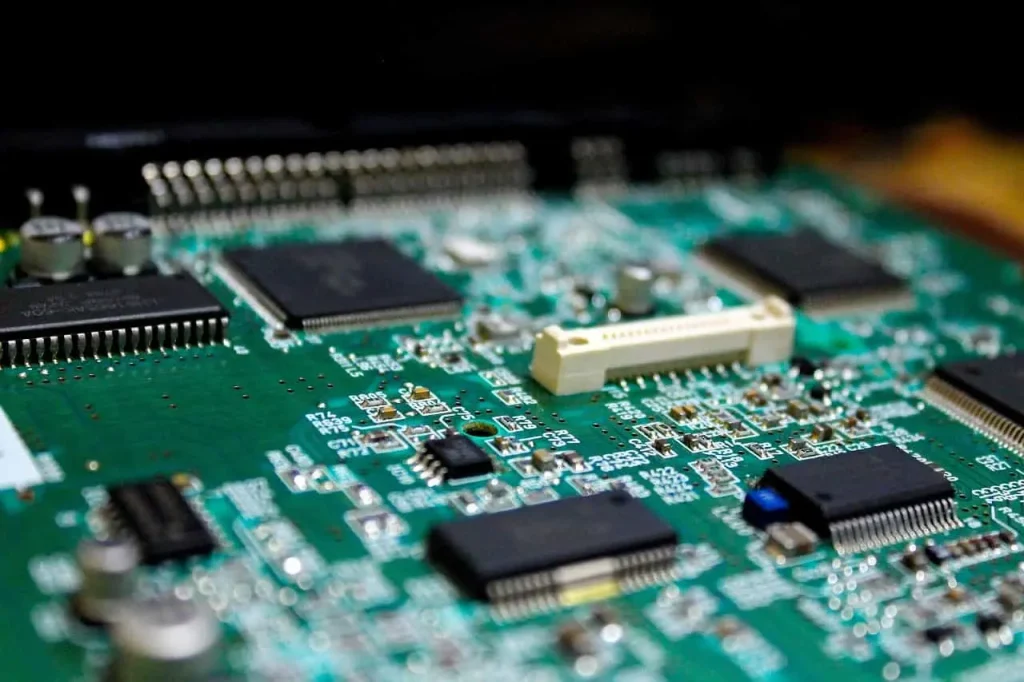
In modern electronics manufacturing, PCBs (Printed Circuit Boards) are the core foundation of nearly all electronic products and are widely used across consumer electronics, automotive systems, industrial control, and communication devices. As products move from the prototype stage into mass production, the focus shifts from whether a single board can be manufactured to how to achieve stable, efficient, and cost-effective large-scale production. High volume PCB assembly has emerged as a key industrial manufacturing model in response to this demand. It relies on automated equipment and standardized processes to achieve large-scale, consistent output, ensuring product quality stability and continuous delivery capability.
Concept and Key Features of High Volume PCB Assembly
High volume PCB assembly refers to a manufacturing process where thousands or even hundreds of thousands of PCBs are continuously assembled, soldered, and tested under industrial production conditions. Its core value lies in achieving highly consistent replication through standardized processes.
- High level of automation: The production process relies on high-speed pick-and-place machines, solder paste printing systems, and reflow soldering equipment, with minimal manual involvement.
- Standardized process control: Parameters such as solder paste thickness, component placement position, and reflow temperature are kept consistent to ensure uniform results across batches.
- Strong product consistency: PCBs produced on the same line have minimal variation in solder joint quality and structural performance.
- Lower unit cost with scale: Increased production volume improves material procurement efficiency and spreads fixed costs, reducing overall manufacturing cost.
- Full traceability system: Each batch is fully recorded, enabling efficient quality tracking and production management.
Key Process Comparison in High Volume PCB Assembly
| Process Stage | Function | Key Characteristics | Application Scope |
| Solder Paste Printing | Provides solder material foundation | High-precision stencil control | SMT assembly |
| Pick and Place | Places electronic components | Fully automated high-speed operation | Resistors, capacitors, ICs |
| Reflow Soldering | Bonds SMT components | Strict temperature profile control | Surface mount structures |
| Wave Soldering | Solders through-hole components | Suitable for THT structures | Through-hole PCBs |
| AOI Inspection | Detects visual defects | Non-contact optical inspection | Full production line |
| X-ray Inspection | Analyzes internal solder joints | Detects BGA hidden joints | High-density packages |
| Functional Testing | Verifies electrical performance | Simulates real operating conditions | Final product testing |
Production Workflow of High Volume PCB Assembly
High volume PCB assembly is a systematic industrial process where each stage directly impacts final product quality.
During the design stage, manufacturability analysis is conducted to ensure that the PCB layout and component placement are suitable for automated production. The bill of materials is also reviewed to avoid mismatches during mass production.
- Solder paste printing: A stencil is used to apply solder paste evenly onto PCB pads, providing a stable foundation for component mounting.
- Component placement: High-speed pick-and-place machines accurately position resistors, capacitors, and integrated circuits according to programmed coordinates.
- Soldering process: Depending on the structure, either reflow soldering or wave soldering is used to form stable electrical connections, with strict temperature profile control.
- Automatic Optical Inspection (AOI): Used to detect component misalignment, missing parts, and soldering defects.
- X-ray inspection: Used to analyze hidden solder joints such as BGA structures and detect internal defects.
- Functional testing (FCT): Verifies electrical performance under powered conditions to ensure design compliance.
- Cleaning and protection: Residual flux is removed, anti-static packaging is applied, and products are managed by batch tracking.
Core Advantages of High Volume PCB Assembly
High volume PCB assembly plays an essential role in the electronics manufacturing ecosystem due to its balanced performance in cost, efficiency, and quality.
- Optimized cost structure: Large-scale procurement and improved equipment utilization reduce per-unit manufacturing cost.
- Improved production efficiency: Automated production lines operate continuously, enabling high output and fast delivery cycles.
- Higher quality stability: Standardized equipment and processes reduce human error and ensure consistent product quality.
- Strong supply capability: Suitable for products requiring continuous and stable mass production, such as consumer electronics and automotive systems.
Application Areas of High Volume PCB Assembly
High volume PCB assembly is widely used across multiple industries and has become a fundamental part of modern electronics manufacturing.
- Consumer electronics: Smartphones, tablets, and wearable devices rely heavily on mass production efficiency.
- Automotive electronics: Control modules, battery management systems, and in-vehicle communication systems require high reliability and stable output.
- Industrial control systems: Long-term operating equipment requires strong consistency and durability.
- Communication and medical devices: Play a key role in large-scale deployment and high-reliability environments.
- IoT devices: Large volumes of standardized devices depend on scalable PCB production.
Future Trends: Moving Toward Smart Manufacturing
As electronics manufacturing continues to evolve, high volume PCB assembly is shifting toward digitalization and intelligent production systems.
- Increased adoption of AI inspection: Algorithms improve defect detection accuracy and efficiency.
- Deep MES integration: Enables real-time monitoring and full-process traceability of production data.
- Advancements in high-density PCB technology: HDI and miniaturized components demand higher assembly precision.
- More data-driven manufacturing: Production control is shifting from experience-based to data-driven decision-making.
In the rapidly growing global electronics industry, high volume PCB assembly has become an indispensable part of the manufacturing ecosystem. It not only determines production efficiency and cost structure but also directly impacts delivery capability and market competitiveness. For electronics manufacturers, building a stable and reliable high volume PCB assembly capability is a critical foundation for achieving scalable production and long-term development.