


Professional Low Volume PCB Assembly (1–5000 Boards)
We provide high-quality low volume PCB assembly services, specializing in production runs from 1 to 5000 boards. This service is ideal for prototyping, pilot production, and early-stage manufacturing where flexibility, precision, and fast turnaround are critical.
Our one-stop turnkey solution covers the entire process, including:
· PCB fabrication
· Component sourcing
· SMT / DIP assembly
· Testing and quality assurance
· Final inspection and delivery
For every project, we strictly perform DFM (Design for Manufacturability) and DFA (Design for Assembly) reviews. This ensures the optimal balance between:
· Product quality
· Manufacturing cost
· Lead time efficiency
By combining engineering expertise with global supply chain integration, we help customers accelerate product development while maintaining full control over cost and performance.
Core Capabilities
Our manufacturing system is designed to support complex designs and diverse industry requirements. We not only focus on assembly but also provide engineering-driven optimization throughout the production lifecycle.
Key Capabilities
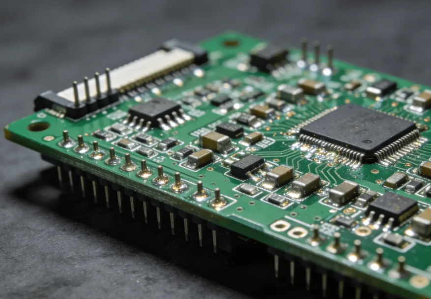
· SMT & DIP mixed assembly for flexible production
· Support for multilayer PCBs, HDI, and complex structures
· Global component sourcing to minimize shortage risks
· Fast prototyping and small batch production
· Support for fine-pitch components and BGA packages
These capabilities allow us to serve industries such as:
· Industrial control systems
· Medical electronics
· Automotive electronics
· Communication equipment
· Consumer electronics
Service Overview
| Item | Details |
| Production Volume | 1–5000 boards |
| Service Type | Turnkey PCBA |
| Assembly Process | SMT / DIP |
| Inspection Methods | AOI, ICT, Functional Testing, X-Ray |
| Testing Standard | 100% Electrical Testing |
DFM (Design for Manufacturability) | Prevent Issues at the Source
DFM is a critical step in low volume PCB assembly. Poor manufacturability can lead to production delays, increased costs, and low yield rates.
We conduct a comprehensive engineering review, including:
· Gerber files
· Bill of Materials (BOM)
· Assembly drawings
· Circuit schematics
Key DFM Optimization Areas
· PCB panelization to reduce cost and improve throughput
· Solder mask opening optimization to prevent solder bridging
· Pad size and spacing validation
· BOM consistency and accuracy check
· Component availability and lifecycle assessment
(Effective DFM analysis helps reduce rework, improve yield, and ensure smooth production.)
DFM Checkpoints Table
| DFM Item | Check Content | Benefit |
| Solder Mask | Clearance & opening accuracy | Prevents solder defects |
| Pad Design | Size, spacing, geometry | Improves solder reliability |
| Panelization | Board layout optimization | Reduces cost |
| File Match | BOM vs Gerber alignment | Avoids mismatch |
| Footprint | Package verification | Ensures correct assembly |
DFA (Design for Assembly) | Improve Efficiency
In addition to manufacturability, DFA focuses on assembly efficiency and testing accessibility.
We assist customers during the design stage to optimize:
· Test point layout
· Fixture and probe selection
· Assembly sequence
· Testing workflow
Proper DFA design reduces assembly complexity and improves production speed.
DFA Support
| Item | Description |
| Test Point Optimization | Improve test coverage |
| Testing Methods | ICT / Functional Testing |
| Engineering Support | Debugging and failure analysis |
Quality Control System
Quality is at the core of our PCB assembly services. Every PCB undergoes strict inspection and testing procedures to ensure performance and reliability.
Inspection & Testing Methods
- Automated Optical Inspection (AOI)
- In-Circuit Testing (ICT)
- Functional Testing (FCT)
- Multi-stage visual inspection
- X-ray inspection (for BGA and complex packages)
Testing Methodology Overview
| Test Method | Purpose | Application Scenario |
| AOI | Detect visual defects | SMT assembly |
| ICT | Verify electrical performance | Circuit validation |
| Functional Test | Simulate real conditions | Product verification |
| X-Ray | Inspect hidden joints | BGA/QFN |
| Visual Inspection | Final manual check | Quality assurance |
All boards undergo 100% electrical testing to guarantee reliability before shipment
Value-Added Services
To ensure a smooth and risk-free production experience, we provide additional engineering and validation services.
PCB Prototype Program
Before full production:
· A small batch of assembled boards is delivered
· Customers can perform real-world testing
· Production begins only after approval
Benefits of This Approach:
· Reduce production risk
·Minimize rework cost
·Improve product reliability
·Accelerate time-to-market
Cost Optimization
Cost efficiency is essential in low volume production. We implement multiple strategies to ensure competitive pricing.
Key Cost Advantages
- No NRE (Non-Recurring Engineering) fees for repeat orders
- Free stencil/tooling for returning customers
- Optimized component sourcing strategies
- Global supplier partnerships
Cost Optimization Table
| Cost Factor | Our Strategy | Customer Benefit |
| Component Pricing | Bulk negotiation | Lower cost |
| Repeat Orders | No NRE fees | Long-term savings |
| Supply Chain | Global sourcing | Stable supply |
| Efficiency | Process optimization | Faster turnaround |
Why Choose Our PCB Assembly Services?
Choosing the right PCB assembly partner is critical for product success. We offer:
·One-stop turnkey PCBA solution
·Strong DFM + DFA engineering capability
·Support for complex PCB designs and packages
·Stable quality with fast delivery
·Competitive pricing for low volume production
Our goal is not just to manufacture your boards, but to optimize your entire product development process.
Get a Quote
To receive an accurate quotation, please provide:
·Bill of Materials (BOM)
·Gerber files
Email: sales@toplinecircuit.com
What You Will Get?
·Detailed engineering review
·Identification of potential issues
·Transparent and competitive pricing
·Professional optimization suggestions