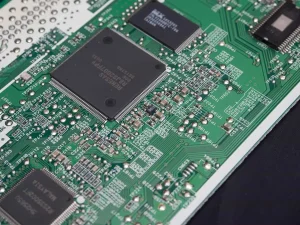
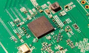
As signal frequencies increase, signal amplitude gradually decreases and may even become distorted during transmission due to conductor loss, dielectric loss, and discontinuous structures. This attenuation not only affects the accuracy of data transmission but can also lead to an increase in the system’s bit error rate, and in severe cases, even communication failure. Therefore, taking effective measures to reduce signal attenuation during the design phase is crucial for ensuring the stable operation of high-speed circuits. Signal attenuation mainly comes from two aspects: conductor loss caused by the resistance and surface roughness of the conductor itself, and energy loss of the PCB dielectric material at high frequencies. Furthermore, unreasonable routing methods, excessive vias, and impedance discontinuities can further exacerbate signal attenuation.
Key Measures to Reduce Signal Attenuation
· Select Low-Loss Materials
Using materials with low dielectric loss (low Df), such as high-frequency specialized substrates, can significantly reduce energy loss during signal transmission.
· Control Trace Length
The longer the signal path, the more significant the attenuation; therefore, signal trace distances should be minimized.
· Optimize Impedance Matching
Maintaining continuous transmission line impedance avoids additional losses caused by reflections.
· Reduce Vias Number
Vias introduce parasitic effects, increasing signal loss. Vias should be minimized or optimized as much as possible.
· Improve Copper Surface Quality
Using low-roughness copper foil can reduce skin effect loss at high frequencies.
· Optimize Stack-Up Structure
By optimizing the stack-up structure, the signal is brought closer to the reference plane, reducing radiation and loss.
Differences in Effectiveness of Different Methods
Different strategies have varying effects on reducing signal attenuation. For example, simply shortening trace length is simple but often difficult to fully achieve in complex circuits. In contrast, choosing low-loss materials, although more expensive, is more effective in high-frequency applications. Furthermore, reducing vias and optimizing impedance matching are structural optimization methods that can improve signal quality without significantly increasing cost, while replacing materials with high-end ones is more commonly used in high-performance products. While there is little difference between ordinary copper foil and low-roughness copper foil at low frequencies, the latter can significantly reduce loss in high-speed environments.
Frequently Asked Questions
Q: What is the difference between signal attenuation and signal reflection?
A: Attenuation is the reduction of signal energy, while reflection is the signal returning due to impedance mismatch.
Q: Why are high-frequency signals more prone to attenuation?
A: Because conductor loss and dielectric loss increase at high frequencies.
Q: Why do vias affect signal strength?
A: Vias introduce parasitic inductance and capacitance, affecting signal transmission.
Q: Are low-loss materials always better?
A: They offer better performance but are more expensive, and the choice depends on project requirements.
Practical Application Examples
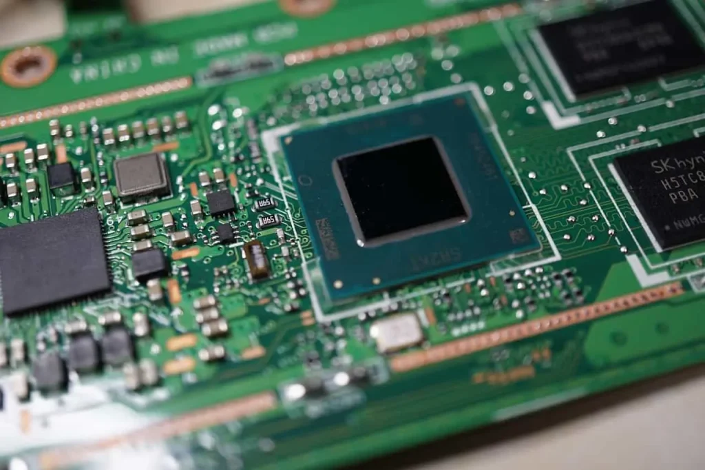
For example, in high-speed communication equipment, such as server motherboards or network switching equipment, signal rates often reach GHz levels. Using ordinary FR-4 materials in these situations can lead to significant signal attenuation. Therefore, engineers typically choose low-loss materials and strictly control trace length and impedance. Signal attenuation is even more pronounced in RF circuit design. For instance, in microwave applications, excessively rough copper surfaces significantly increase losses. Therefore, high-quality copper foil and optimized manufacturing processes are usually employed. In these high-end applications, companies like Topray Circuits can provide a variety of solutions, including RF PCBs and HDI boards, effectively reducing signal attenuation and improving product performance through optimized materials and processes.
In high-speed PCB design and manufacturing, signal attenuation control often manifests as the cumulative effect of multiple details, rather than a single change. For example, seemingly basic design choices such as whether traces are as straight and short as possible, whether unnecessary vias are avoided, and whether reference planes are continuous, all have a lasting impact on final signal quality. Simultaneously, material selection is equally crucial, especially in high-frequency applications, where low-loss dielectrics and high-quality copper foil can reduce energy loss at the source. Furthermore, the stability of the manufacturing process cannot be ignored. Even with a reasonable design, improper parameter control during production can still lead to signal performance degradation. Therefore, considering design and manufacturing in tandem has become an important approach in current high-speed PCB development. In this process, companies like Topray Circuits, by integrating PCB layout, manufacturing, assembly, and testing capabilities, can optimize multiple stages simultaneously, thereby reducing error accumulation and improving overall signal performance.