


As display modules, touch modules, high-definition camera assemblies, and high-speed control terminals continue to evolve toward thinner, lighter, and more integrated designs, double-sided impedance FPCs have become a very important flexible circuit solution for high-frequency and high-speed interconnection applications. These circuits must not only meet the basic requirements of flexible circuit boards—such as bendability and cross-space interconnection—but also maintain stable impedance control during high-speed signal transmission, minimizing attenuation, reflection, crosstalk, and poor contact risks. For applications such as 4K displays, high-speed touch signals, precision control signals, and multi-channel display modules, the value of a double-sided impedance FPC lies not only in “conductivity,” but in ensuring that signals remain stable, clear, and continuous even within complex structures.
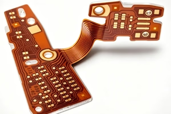
Double-sided impedance FPCs are commonly used in electronic devices that demand extremely compact space utilization and very strict signal integrity requirements. They route circuits on both sides of the flexible substrate while achieving high-density interconnection through vias, coverlays, and fine-line circuit design. Compared with ordinary flexible boards, they place greater emphasis on impedance consistency, circuit precision, via accuracy, and surface treatment stability, making them more suitable for products requiring excellent video quality, touch responsiveness, and high-speed data transmission.
Basic Concept: What is a Double-sided Impedance FPC?
Basic definition of a double-sided impedance FPC
A double-sided impedance FPC is a flexible printed circuit board with conductive traces formed on both sides of the flexible substrate, while the impedance of the circuit is precisely controlled during design and manufacturing. It is not simply a matter of routing traces on two sides; instead, the design must carefully control line width, spacing, copper thickness, dielectric thickness, via structure, and surface treatment to ensure stable electrical characteristics during high-speed signal transmission. For applications such as high-definition video, touch signals, and high-speed display interfaces, impedance stability directly determines signal clarity, display smoothness, and system immunity to interference.
Why high-speed signal transmission requires impedance control?
The biggest difference between high-speed signals and ordinary low-speed signals is that high-speed signals are extremely sensitive to changes in the transmission environment. Even small impedance deviations can cause reflections, waveform distortion, timing errors, and increased crosstalk. Especially in high-resolution display modules or high-speed touch systems, the higher the signal frequency, the stricter the requirements for transmission consistency. Therefore, a double-sided impedance FPC is not simply “a regular FPC with traces on both sides,” but rather a flexible circuit solution designed for much higher signal stability standards.
Main features and specifications
| Main Feature | Technical Specification | Core Advantage |
| Surface finish | ENIG (Electroless Nickel Immersion Gold) | Enhances oxidation resistance and solderability, reduces long-term contact resistance, and ensures stable interface connections. |
| Outer layer copper thickness | 35μm | Minimizes signal attenuation during transmission, supports high-definition video (such as 4K) and high-speed touch signal transmission, and avoids signal distortion. |
| Circuit precision | Minimum line width/spacing: 4/4mil; minimum via size: 0.25mm | Supports high-density circuit layouts, adapts to multi-signal channel display module designs, and reduces circuit interference. |
| HDI design | Mechanical via density: 2 vias/cm² | Meets the routing requirements of highly integrated display devices, optimizes signal paths, and reduces crosstalk risk. |
| Solder mask and silkscreen | Yellow solder mask + white silkscreen | Clear silkscreen markings facilitate positioning and inspection during assembly; the yellow solder mask improves visual recognition and scratch resistance. |
| Via protection | Coverlay-covered vias | Isolates dust and moisture, prevents via corrosion, extends product lifespan, and improves reliability in harsh environments. |
Application range
Double-sided impedance FPCs are ideal for products that require “limited space, high signal quality, and complex structures.” Common applications include display modules, 4K high-definition video equipment, touch-screen control components, portable terminals, precision sensor interconnections, mixed power-and-signal transmission modules, and other electronic products requiring high-density flexible interconnection. Their core value lies in providing more stable electrical connections and stronger structural adaptability without increasing overall product size.
How is a Double-sided Impedance FPC Made?
Requirement confirmation and signal planning
The design process begins with defining application requirements rather than simply determining board dimensions. Engineers must clarify whether the product will carry 4K display signals, touch signals, or mixed multi-channel signals; determine required data rates; identify whether traces pass through bending areas; and evaluate space limitations and dual-side component coordination. Only after fully understanding the application scenario can impedance design, stack-up configuration, via quantity, and protection methods be optimized properly. For high-speed signal products, accurate early-stage definition significantly reduces the risk of redesign later.
Stack-up design and impedance calculation
Achieving stable impedance in a double-sided FPC depends heavily on stack-up structure design. Flexible substrate thickness, copper thickness, coverlay thickness, and reference plane arrangement all influence final impedance values. During design, simulation and manufacturing capability evaluations are used repeatedly to optimize line width, spacing, and dielectric thickness so that target impedance values remain within tolerance. Especially in高速 signal channels, inconsistent impedance between top and bottom routing layers can create reflection points and negatively affect the entire signal chain.
Circuit fabrication and via processing
Double-sided FPCs require circuits on both sides of the substrate with vias providing electrical interconnection. Because flexible materials are thin and soft, drilling accuracy, via plating quality, and layer alignment precision are critical. In particular, a minimum via size of 0.25mm places high demands on manufacturing capability and yield control. Through via protection, coverlay openings, and precision plating control, vias can remain stable during long-term use and resist moisture and contamination.
Surface treatment and finished product testing
ENIG surface treatment provides stable, flat, and oxidation-resistant surfaces for pads and connector areas, making it highly suitable for products with strict soldering reliability and long-term contact performance requirements. After manufacturing, products undergo continuity testing, impedance testing, visual inspection, and bending verification to ensure circuits meet design standards. For high-speed signal products, testing is not only about conductivity, but also about signal stability.
| Manufacturing Step | Function |
| Requirement confirmation | Defines signal type, space limitations, and bending conditions |
| Stack-up design | Establishes stable impedance and reference paths |
| Circuit formation | Creates fine-line routing on both sides |
| Via processing | Achieves interconnection between both layers |
| Surface treatment | Improves solderability and oxidation resistance |
| Electrical testing | Verifies conductivity and impedance performance |
How to Optimize a Double-sided Impedance FPC?
Impedance control is the core
The key value of a double-sided impedance FPC is not just “flexibility,” but “stable impedance.” When high-speed signals encounter impedance fluctuations, waveform distortion and data errors may occur. Therefore, line width, spacing, copper thickness, dielectric thickness, and reference planes must all be strictly controlled. For differential signals, line length, spacing, and surrounding environments should remain as consistent as possible to ensure balanced transmission and strong anti-interference performance.
Significance of 35μm outer copper thickness
An outer copper thickness of 35μm helps reduce transmission loss, improve conductivity, and enhance mechanical stability. For high-definition video and high-speed touch signals, this thickness minimizes attenuation and maintains clearer data transmission. However, thicker copper also creates challenges in flexibility and process control, so conductivity and bending performance must be balanced carefully.
Importance of 4/4mil line width/spacing and 0.25mm vias
A minimum line width/spacing of 4/4mil indicates high circuit precision suitable for dense routing and multi-channel signal designs. This precision allows engineers to place more signal channels within limited space while controlling crosstalk. A minimum via size of 0.25mm supports more compact interconnection structures, but also demands higher drilling, plating, and alignment precision. High precision enables high density, which in turn requires highly stable manufacturing processes.
HDI design and crosstalk suppression
When mechanical via density reaches 2 vias/cm², the board enters a high-density interconnect design stage. To minimize crosstalk and signal interference, engineers optimize routing paths, shorten critical signal lengths, reduce unnecessary layer transitions, and improve reference plane integrity when necessary. For multi-channel products such as display modules, HDI design significantly improves routing flexibility but also requires stricter process control.
Functions of solder mask, silkscreen, and coverlay
Yellow solder mask and white silkscreen improve visual recognition and make assembly positioning and inspection easier. Coverlay-protected vias prevent dust and moisture from damaging via structures, thereby extending product lifespan. This type of protection is especially important in flexible circuits because FPCs are often used in compact and moving structures where environmental exposure can affect long-term reliability.
Key technical optimization table
| Technical Direction | Optimization Method | Target Effect |
| Impedance control | Precise control of line width, spacing, and dielectric thickness | Stable high-speed signal transmission |
| Copper thickness management | 35μm outer copper thickness | Reduced signal attenuation |
| High-density routing | 4/4mil fine-line circuits | Improved integration density |
| Via protection | Coverlay-covered vias | Moisture and dust protection, extended lifespan |
| HDI layout | Controlled via density | Reduced crosstalk risk |
What Materials Should Be Used for Double-sided Impedance FPCs?
Flexible substrate selection
The most commonly used flexible substrate for double-sided impedance FPCs is polyimide (PI). PI offers excellent heat resistance, flexibility, and dimensional stability, making it highly suitable for high-speed flexible circuits. In areas requiring bending or cross-space routing, PI provides strong mechanical durability while helping maintain impedance consistency.
Conductor material selection
Conductors are typically made from high-quality copper foil. In demanding high-speed transmission applications, copper thickness, copper quality, and adhesion strength are all critical. The 35μm outer copper thickness must balance conductivity, flexibility, and process compatibility, taking into account signal loss, bending lifespan, and manufacturing stability.
Surface treatment and protective materials
ENIG surface treatment is ideal for products requiring strong solderability, oxidation resistance, and long-term connection stability. Coverlays protect circuits, vias, and flexible areas from external damage. The combination of yellow solder mask and white silkscreen also improves visual identification, inspection, and assembly accuracy.
| Material Area | Common Material | Function |
| Flexible substrate | PI (Polyimide) | Heat resistance, flexibility, dimensional stability |
| Conductor material | Copper foil | Signal transmission and conductivity |
| Surface finish | ENIG | Oxidation resistance and solderability |
| Protective layer | Coverlay | Dust and moisture protection, via protection |
| Marking layer | Yellow solder mask + white silkscreen | Easy identification and assembly |
Material selection
A high-speed signal transmission double-sided impedance FPC cannot be optimized simply by selecting “more expensive” materials. Material choices must match actual application requirements. Display modules focus more on signal integrity and multi-channel transmission, touch modules emphasize response stability and thinness, while industrial equipment values durability and anti-interference capability. Material selection should align with these real-world requirements to maximize FPC performance advantages.
Why are Double-sided Impedance FPCs More Suitable for High-speed Display and Touch Products?
Many customers ask why high-speed display and touch products are better suited to double-sided impedance FPCs instead of ordinary flexible circuits. The answer is simple: high-speed signals are extremely sensitive to transmission conditions. Without strict impedance control, ordinary flexible circuits may suffer from display lag, signal attenuation, poor touch responsiveness, or insufficient anti-interference performance. Through double-sided routing, high-precision line control, ENIG surface treatment, via protection, and HDI design, double-sided impedance FPCs create more stable signal transmission paths within limited space. They meet the transmission requirements of high-speed video and multi-channel data while adapting to complex installation structures and bending spaces, making them ideal for HD displays, smart terminals, precision touch systems, and multi-signal integrated devices.
Why Choose Us for Custom Double-sided Impedance FPCs for High-speed Signal Transmission?
We specialize in providing double-sided impedance FPC solutions optimized for high-speed signal transmission. Whether for display modules, touch systems, or other products requiring excellent signal integrity, we can customize designs according to your routing precision, impedance targets, structural space, and material requirements. For 4K displays, high-speed touch signals, and high-density multi-channel transmission scenarios, we focus on overall system stability rather than isolated specifications. Through optimized stack-up design, strict process control, and suitable material selection, we help customers reduce trial-and-error during product development and achieve smoother mass production.
Double-sided impedance FPCs designed for high-speed signal transmission solve more than just the problem of “flexible interconnection.” They solve the challenge of maintaining stable, clear, and low-loss signal transmission within complex spaces. For display modules, touch modules, and precision electronic devices, their value lies in achieving miniaturization, lightweight construction, and high performance simultaneously. Double-sided routing improves circuit utilization efficiency; impedance control stabilizes signal transmission; and ENIG surface treatment, coverlay protection, and precision manufacturing ensure long-term reliability.
For companies, this type of FPC not only enhances product performance but also reduces maintenance and repair risks. If your project requires a more suitable flexible circuit solution for high-speed signal transmission, feel free to send us your drawings, specifications, and application requirements. We will provide tailored design recommendations and quotation support to help you complete development faster and move smoothly into mass production.


")

