


Double-sided PCBs are increasingly used in consumer electronics, industrial control, LED lighting, and communication equipment, and the surface finish process directly affects PCB soldering quality, long-term reliability, and manufacturing cost. Among various surface finish solutions, OSP (Organic Solderability Preservative) has become an important choice in double-sided PCB manufacturing due to its good solderability, flatness, and environmental friendliness. Compared with traditional HASL and some metal plating processes, OSP surface finish effectively reduces manufacturing costs while meeting the requirements of high-density assembly and fine-pitch component soldering. Through proper circuit design, impedance control, and surface finish process optimization, custom double-sided PCBs with OSP surface finish can improve overall soldering stability and meet the development demands of electronic products for thinness, high integration, and environmental friendliness.
Custom OSP Surface Finish Double-Sided PCB Product Introduction
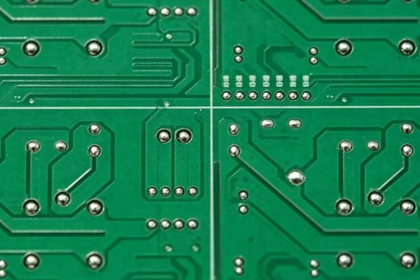
OSP surface finish double-sided PCBs are double-layer printed circuit boards using an organic protective film process, widely used in consumer electronics, LED lighting, industrial control, communication equipment, and other fields. The OSP process forms an ultra-thin organic protective film on the copper surface to prevent copper oxidation and ensure the PCB maintains good solderability during storage and transportation. During high-temperature soldering, the OSP protective film rapidly decomposes and volatilizes, exposing a clean copper surface, allowing the solder to form a stable bond with the copper layer. Compared with some traditional surface finish processes, OSP offers better surface flatness, lower manufacturing costs, and more environmentally friendly process characteristics, making it more suitable for fine-pitch assembly and high-density PCB design requirements.
Custom OSP Surface Finish Double-Sided PCB Product Advantages
Modern electronic products have increasingly stringent requirements for PCB soldering performance and manufacturing cost.
- The OSP process effectively reduces surface finish manufacturing costs, making it suitable for high-volume PCB production projects.
- Compared with some metal plating processes, the OSP process flow is simpler, helping to shorten manufacturing lead times.
- The high flatness of OSP surface finish makes it more suitable for BGA, QFN, and fine-pitch component assembly.
- High flatness reduces issues such as cold solder joints, bridging, and uneven soldering.
- The OSP film decomposes quickly during soldering, forming a clean copper surface and improving soldering reliability.
- Environmentally friendly organic protective film complies with RoHS, REACH, and other environmental requirements.
- Double-sided PCB structure improves wiring flexibility and space utilization.
- Supports high-density circuitry and complex circuit layout designs.
Good solderability and manufacturing economy are key advantages of OSP double-sided PCBs.
Why Choose Our Custom OSP Surface Finish Double-Sided PCB Products
Double-sided PCB manufacturing places stricter requirements on circuit accuracy and surface finish stability.
- We support customization of OSP double-sided PCBs, multilayer PCBs, and high-density structures.
- High-precision etching and impedance control processes ensure circuit stability and signal integrity.
- We support fine line width and spacing, high-density assembly, and complex circuit layout designs.
- Copper thickness, board thickness, and special process solutions can be customized according to project requirements.
- We support various surface finish options including OSP, ENIG, and HASL.
- With extensive experience in double-sided PCB manufacturing, we are suitable for consumer electronics and industrial applications.
- We support high-Tg materials and high-reliability structural designs.
- Strict control of surface flatness and soldering consistency improves product stability.
Mature manufacturing processes and flexible customization capabilities make it easier to meet complex double-sided PCB project requirements.
Custom OSP Surface Finish Double-Sided PCB Product Frequently Asked Questions
During the development phase, many projects pay special attention to the actual performance of OSP surface finish.
- Compared with ENIG, OSP surface finish offers lower manufacturing costs.
- The high flatness structure is more suitable for high-density SMT assembly environments.
- The OSP process leaves almost no residue after soldering, improving soldering cleanliness.
- The organic protective film effectively prevents copper surface oxidation during storage.
- Under multiple high-temperature reflow soldering cycles, proper process parameters need to be controlled.
- Double-sided PCB structure improves circuit layout flexibility and space utilization.
- The OSP process aligns with environmentally friendly manufacturing directions, suitable for green electronic product projects.
- Proper impedance control and circuit design improve overall electrical stability.
Solderability and long-term stability are important considerations for OSP double-sided PCBs.
Custom OSP Surface Finish Double-Sided PCB Product Main Features
Electronic equipment has continuously increasing requirements for PCB flatness and high-density assembly capability.
- OSP double-sided PCBs support fine-pitch, high-density, and complex circuit design environments.
- The high flatness surface is more suitable for precision component soldering such as BGA and QFN.
- Supports high-frequency, high-speed, and high-reliability PCB design solutions.
- Double-sided circuit structure improves overall circuit integration capability.
- The OSP protective film decomposes rapidly during soldering, achieving a clean copper surface bond.
- Applicable to consumer electronics, LED lighting, industrial control, and various other application fields.
- Environmentally friendly process aligns with the development direction of modern electronics manufacturing.
- Supports various special process and structural customization requirements.
Flexible structural design enables OSP surface finish double-sided PCBs to meet the needs of various electronic systems.
Application Areas
| Application Direction | Main Requirement | PCB Characteristic |
| Consumer Electronics | High-density assembly | High flatness |
| LED Lighting | Soldering stability | OSP protective layer |
| Industrial Control | Long-term operation | High reliability |
| Communication Equipment | Signal stability | Impedance control |
| Power Module | Cost control | Manufacturing economy |
| Smart Devices | Miniaturized design | Double-sided wiring |
The development of custom OSP surface finish double-sided PCB design is driving electronic products toward higher integration, better soldering stability, and greater environmental friendliness. In consumer electronics, industrial control, LED lighting, and communication systems, OSP double-sided PCBs have become an important foundational solution that balances manufacturing cost, solderability, and structural flexibility. Facing high-density assembly, complex circuit layout, and environmentally friendly manufacturing requirements, PCBs must achieve a more reasonable balance among materials, surface finish, manufacturing processes, and structural design. Through systematic analysis of product advantages, manufacturing capabilities, frequently asked questions, and main features, we can more fully understand the application value of OSP surface finish double-sided PCBs in modern electronic systems, and provide clearer reference directions for subsequent product development and solution design.
If you need assistance, please contact us at sales@toplinecircuit.com.


")

