


Custom impedance controlled PCB is the core of signal transmission in communication equipment. It can accurately adapt to high-frequency scenarios such as GPS and satellite communication, solve problems of signal reflection and loss, provide support for stable operation of equipment, and meet the customization needs of various communication equipment.
Core Product Advantages
To meet the core needs of signal transmission in communication equipment (including GPS and satellite communication equipment), our custom impedance controlled PCB has four core advantages, comprehensively ensuring the stability and adaptability of equipment operation.
- Precise Impedance: Adopting LDI technology, the impedance deviation is controlled within ±3%, matching 50Ω, 75Ω, and 100Ω standards, suitable for GPS modules and satellite communication high-frequency signal transmission.
- High-Quality Material: Selected high-frequency and low-loss circuit boards, resistant to complex environments, supporting aerospace-grade material customization to meet the needs of satellite communication in extreme environments.
- Flexible Customization: The number of PCB layers, line width, etc., can be adjusted according to equipment size and signal rate, suitable for various equipment from small GPS terminals to large satellite ground stations.
- Reliable Quality: Implemented IPC-6012 Class 3/3A standards, strictly inspected throughout the whole process to ensure the consistency of mass production and reduce the risk of equipment failure.
The above advantages can accurately match high-frequency scenarios such as GPS and satellite communication, providing stable and efficient PCB support for various communication equipment and helping equipment exert optimal performance.
Main Product Features
| Feature Category | Specific Description |
| High-Frequency Optimization | Optimized RF wiring for GPS and satellite communication, reducing signal attenuation and adapting to satellite communication Ka and V band signals. |
| Strong Anti-Interference | Multi-layer design with independent ground/power layers, shielding impedance lines to avoid crosstalk between GPS signals and other signals. |
| Efficient Process | Adopting advanced technologies such as laser drilling to improve precision, shorten cycles, and adapt to the miniaturization needs of communication equipment. |
| Technical Support | Provide one-on-one technical docking from design simulation to mass production to solve various application problems. |
Frequently Asked Questions
Q1: Can it adapt to the miniaturization needs of GPS navigation equipment?
A1: Yes, ultra-thin and miniaturized PCBs can be customized, using blind/buried via technology to reduce volume without affecting GPS signal transmission.
Q2: Can it withstand extreme environments in satellite communication equipment?
A2: Yes, aerospace-grade materials are selected and processes are optimized, which can withstand -40℃~125℃, vacuum and high radiation environments to ensure stable signals.
Q3: How to determine the suitable impedance value?
A3: Professional technicians will dock, combine equipment parameters, and determine the optimal impedance value through simulation calculations to ensure compliance.
Q4: How to verify impedance accuracy?
A4: Each batch is sampled and tested with TDR, test data is provided, and third-party test reports can be provided additionally.
Application Scenarios
Combined with the usage needs of various communication equipment such as GPS and satellite communication, our custom impedance controlled PCB covers multiple scenarios, specifically as follows:
- GPS Navigation Equipment: On-board, portable, UAV GPS modules, etc., ensuring positioning accuracy.
- Satellite Communication Equipment: Satellite payloads, ground stations, satellite phones, etc., adapting to high-frequency signals and extreme environments.
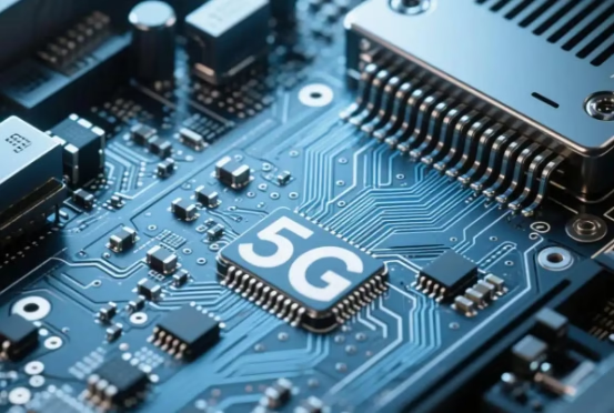
- High-Frequency Communication Equipment: 5G base stations, microwave communication equipment, solving signal reflection and crosstalk problems.
- Special Communication Equipment: Military, marine, and aviation communication terminals, with anti-interference and anti-harsh environment capabilities.
These scenarios can give full play to the advantages of PCB such as impedance control and anti-interference, providing solid guarantee for the stable operation of various communication equipment.


")

