


AI servers, GPU computing platforms, data centers, and edge devices need PCBs with stable high-speed transmission, dense routing, and good thermal performance.
Standard PCB structures often face limits in signal loss, routing space, and impedance control.
High-frequency PCBs help reduce transmission loss. HDI PCBs support finer lines, smaller vias, and more compact layouts.
These PCB structures are widely used in AI hardware where signal integrity, board density, and long-term reliability are important.
What Are High-Frequency and HDI PCBs for AI Applications?
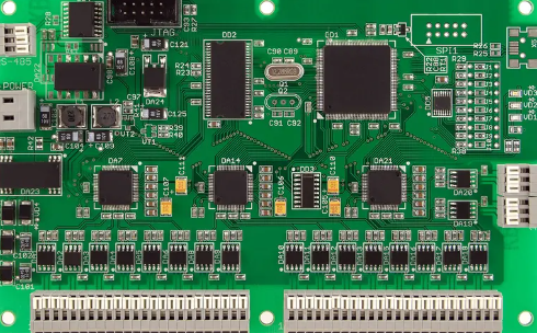
High-frequency and HDI PCBs designed for artificial intelligence applications are high-performance circuit boards specifically developed for high-speed computing, high-frequency signals, and highly integrated electronic systems. These PCBs commonly use microvias, blind and buried vias, multilayer lamination structures, and low-loss high-frequency materials to meet the demanding requirements of AI systems for fast data transmission and stable operation.
Compared with conventional PCBs, these products provide major advantages in signal integrity, routing density, and thermal management.
Key features include:
- High-frequency low-loss design: Reduces signal loss and transmission delay during high-speed operation.
- High-density routing structure: Supports large-scale connections for GPUs, AI chips, and high-speed interfaces.
- Enhanced signal integrity: Minimizes crosstalk, electromagnetic interference, and signal reflection issues.
- Compact PCB size: Improves space utilization for highly integrated devices.
- Improved thermal performance: Optimizes copper layers and structural design for better heat dissipation.
- Support for high-speed interfaces: Compatible with PCIe, DDR, high-speed optical modules, and other advanced interfaces.
Modern AI servers and high-speed computing platforms often require higher-layer HDI structures and stricter impedance control to ensure stable high-speed data operation.
Core Process Comparison of High-Frequency and HDI PCBs
Different manufacturing technologies directly affect PCB performance and application areas. The table below compares common processes used in AI-related high-frequency and HDI PCBs:
| Process Type | Main Function | Technical Features | Typical Applications |
| Laser Microvia Technology | Achieves high-density interconnection | Smaller vias and higher precision | AI server PCBs |
| Blind and Buried Via Process | Improves routing efficiency | Reduces space occupation | High-layer-count HDI PCBs |
| High-Frequency Low-Loss Materials | Reduces signal loss | Improves high-speed signal integrity | GPUs and high-speed computing platforms |
| Sequential Lamination Process | Enhances structural stability | Supports complex stack-up structures | AI computing equipment |
| Impedance Control Technology | Maintains signal stability | Improves transmission consistency | High-speed interface systems |
| Heavy Copper Thermal Structures | Improves thermal management | Enhances heat dissipation efficiency | High-power AI equipment |
AI High-Frequency and HDI PCB Custom Design Process
AI devices require extremely high PCB design precision and electrical performance, making strict engineering and manufacturing control essential during product development.
At the initial design stage, the PCB stack-up structure, high-speed interfaces, and thermal management solutions must be carefully planned according to the AI system architecture.
- PCB stack-up design: Optimizes power layers, ground layers, and high-speed signal layer layouts.
- High-frequency material selection: Chooses low-loss materials based on signal frequency and transmission speed.
- Microvia and HDI structure design: Improves high-density chip connection capability.
- Impedance control analysis: Ensures stable high-speed differential signal transmission.
- Thermal management optimization: Improves cooling performance through copper thickness and heat dissipation structures.
- DFM manufacturability analysis: Enhances production stability and yield rate.
- AOI and X-ray inspection: Detects circuit and internal structural quality.
- Electrical performance testing: Verifies high-speed operational stability.
Advanced AI PCB design often combines high-speed simulation, thermal analysis, and signal integrity optimization to ensure long-term stable operation of complex AI systems.
Why Choose Our AI High-Frequency and HDI PCB Products?
For AI devices, PCBs not only affect computing performance but also directly determine system stability and long-term operational efficiency. High-quality high-frequency and HDI PCB products help customers improve overall AI system performance while reducing long-term operational risks.
- High-precision manufacturing capability: Supports high-layer-count, multi-stage HDI, and ultra-fine routing processes.
- High-frequency and high-speed optimization capability: Reduces signal loss and crosstalk while improving operational stability.
- Enhanced thermal management design: Meets the cooling requirements of high-power AI devices.
- Strict quality control: Uses AOI, X-ray, and impedance testing to ensure product reliability.
- Support for fast prototyping and mass production: Meets the needs of different AI product development stages.
- Extensive industry experience: Suitable for AI servers, data centers, and high-speed communication equipment.
- Stable delivery capability: Optimized supply chain and production management improve product consistency.
Our high-frequency and HDI PCB products are designed to meet the demanding requirements of AI equipment for high-speed, high-frequency, high-density, and highly reliable performance.
Application Areas of AI High-Frequency and HDI PCBs
As artificial intelligence technology continues to evolve, high-frequency and HDI PCBs are now widely used across many advanced industries.
- AI servers: Supports stable operation of GPUs and high-speed computing platforms.
- Data centers: Improves high-speed data exchange efficiency and system stability.
- High-speed networking equipment: Used in switches, routers, and communication systems.
- Autonomous driving systems: Supports onboard AI computing and high-speed data transmission.
- Edge computing devices: Meets compact size and high-performance requirements.
- Medical AI equipment: Improves data processing capability and system reliability.
High-frequency and HDI PCB technology has become an essential foundation for modern AI hardware systems.
Future Trends: AI Drives PCB Technology Toward Higher Frequency and Greater Density
As AI computing demands continue to grow, high-frequency and HDI PCB technology is rapidly advancing. Future PCB manufacturing will focus more on ultra-low-loss materials, higher-layer-count HDI structures, and higher-precision routing processes, while integrating intelligent manufacturing and automated inspection systems to improve product consistency and production efficiency. Advanced packaging, high-speed interfaces, and AI-assisted PCB design technologies will further expand the application of high-frequency and HDI PCBs in next-generation AI devices.
In modern artificial intelligence equipment, high-frequency and HDI printed circuit boards have become a critical foundation that determines system performance, operational stability, and high-speed data processing capability. They not only meet the demands of AI systems for high speed, high frequency, and high integration density, but also significantly improve system reliability and long-term operational efficiency. For companies pursuing high-performance AI hardware products, choosing high-quality high-frequency and HDI PCB products will become an important step toward improving market competitiveness and driving technological advancement.


")

