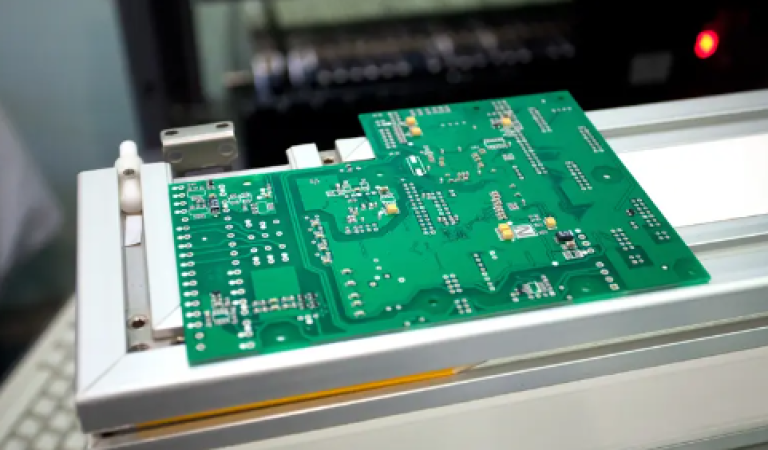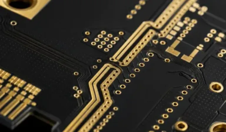

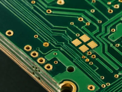
A 4 layer PCB is often selected when a two-layer board does not provide enough routing space or stable reference planes. The additional internal layers can support power and ground distribution while keeping signal routing more organized on the outer layers.
For industrial electronics, the benefit is not simply having more copper layers. The board structure should support the actual needs of the circuit, including power paths, signal routing, connector locations, thermal conditions, and later assembly requirements.
More Space for Signal and Power Routing
A four-layer structure can separate signal traces from internal power and ground planes. This helps reduce routing congestion and gives the designer more flexibility around connectors, controllers, and dense component areas.
Better Ground Reference for Sensitive Signals
An internal ground plane can provide a more stable return path for selected signal traces. This is useful when the board includes communication interfaces, switching circuits, or signals that need more controlled routing.
A Practical Structure for Industrial Boards
Many industrial control boards do not need a complex HDI structure. A well-planned 4 layer PCB can provide a practical balance between routing capacity, electrical requirements, and manufacturability.
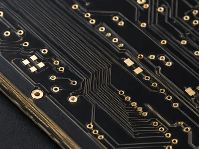
What We Review Before Manufacturing
A 4 layer PCB should be reviewed as a complete fabrication package. Gerber files show the copper pattern, but drill files, board outline data, stack-up notes, and fabrication instructions are also important for confirming the intended board structure.
The review should focus on whether the design can be manufactured as supplied and whether the files clearly communicate the project requirements. This helps prevent unnecessary questions during engineering and quotation preparation.
| Review Area | What Should Be Confirmed |
|---|---|
| Gerber files | Complete top, inner, and bottom layer data |
| Drill files | Hole sizes, slots, vias, and finished-hole notes |
| Layer stack-up | Signal, ground, and power layer arrangement |
| Board outline | Dimensions, cutouts, routes, and mechanical features |
| Material notes | Thermal, electrical, or environment requirements |
| Fabrication drawing | Special instructions and acceptance criteria |
Gerber Files Should Include All Copper Layers
A four-layer board needs complete internal layer data, not only the top and bottom copper. The file package should clearly show the signal, power, and ground layer structure.
Drill and Mechanical Data Need Clear Notes
Drill files should identify through holes, vias, slots, and mechanical cutouts. If a hole or slot has a special function, it should also be stated in the fabrication drawing.
DFM Review Helps Identify Avoidable Issues
DFM review can identify unclear notes, tight drill-to-copper spacing, unusual copper distribution, and layout details that may affect manufacturing. When discussing Gerber preparation and DFM review, link naturally to PCB design.
Layer Stack-Up and Power Distribution
A typical 4 layer PCB often uses outer layers for signal routing and internal layers for power and ground functions. The final arrangement depends on the circuit architecture, routing density, signal requirements, and power distribution needs.
The stack-up should not be treated as a fixed template for every project. Dielectric structure, copper thickness, signal reference, and plane placement should be reviewed from the actual design files.
Internal Ground Plane Planning
A continuous ground plane can help provide a stable reference for selected signal paths. Plane splits, gaps, or unnecessary interruptions should be reviewed when the board includes sensitive routing.
Power Plane and Current Path Review
Internal power layers can support cleaner distribution to multiple circuit sections. High-current paths, thermal areas, and copper balance should be checked before fabrication planning.
Controlled Impedance Requirements
If the board contains impedance-sensitive traces, the target requirements should be supplied with the project files. Trace geometry, dielectric thickness, copper thickness, and stack-up structure must be considered together.
For projects with impedance requirements, use Impedance Controlled PCBs as the relevant internal link.
Material Selection for Industrial Electronics
Material selection should match the operating environment and the electrical requirements of the finished equipment. Standard FR4 can suit many industrial boards, but some projects require further review because of thermal stress, high-frequency signals, or demanding operating conditions.
The material decision should be based on the project requirement, not only on a general material name or expected cost.
Higher Thermal Requirements
Industrial boards used near power devices, motors, converters, or higher-temperature areas may need additional material review. The final material choice should be confirmed from the operating conditions and production requirements.
For higher thermal material considerations, use High Tg PCB as the supporting internal link.
High-Current Routing Requirements
Some industrial electronics need stronger copper paths for power distribution or heat transfer. The copper requirement should be checked together with trace width, plane area, thermal behavior, and layer construction.
For higher-current applications, use Heavy Copper PCBs when the project requirement supports that direction.
Routing and Manufacturing Considerations
A 4 layer PCB can support more organized routing than a two-layer board, but the design still needs to remain practical for fabrication. The board outline, via placement, copper distribution, hole structure, and internal plane arrangement should work together.
Avoiding Unnecessary Layer Complexity
A four-layer structure is suitable for many industrial designs. More layers should only be considered when routing density, signal requirements, component pitch, or power architecture clearly require them.
Checking Copper Balance Across Layers
Large copper areas on one layer and sparse routing on another can affect board flatness and manufacturing balance. Copper distribution should be reviewed before the files are released.
Confirming Board Interfaces Early
Connector areas, mounting holes, edge clearances, and test points should be included in the final Gerber package. These features affect both fabrication and later assembly access.
Preparing for PCB Assembly
A bare 4 layer PCB should be reviewed with the next assembly stage in mind. A board can be ready for fabrication but still create assembly issues if component footprints, pad openings, polarity markings, or test access are unclear.
If the project includes PCB assembly, provide the BOM, pick-and-place file, assembly drawing, and test requirements together with the bare board files.
| Assembly Item | What to Prepare |
| BOM | Manufacturer part numbers and approved alternatives |
| Placement data | Pick-and-place file and component location data |
| Assembly drawing | Polarity, connector, and special assembly notes |
| Test requirements | Test points and functional check requirements |
BOM Review Before Assembly Planning
A complete BOM helps confirm component packages, approved alternatives, and potential sourcing questions. This is especially important when the board includes industrial connectors, power components, or mixed package types.
For BOM review, assembly documentation, and test planning, link naturally to PCBA processing.
Files Required for Quotation
A 4 layer PCB quotation should be based on the complete design package. A board image, layer count, or outline drawing alone does not provide enough information for stack-up and fabrication review.
Please prepare the following files where available:
Preparing Your 4 Layer PCB Project
A 4 layer PCB project should begin with a clear review of the Gerber files, drill data, layer arrangement, material requirements, and power routing needs. The internal layers should support the real electrical and mechanical requirements of the industrial equipment.
Before production planning, confirm that the latest revision includes all fabrication notes and any assembly-related requirements. This helps reduce avoidable engineering questions and supports a smoother transition into PCB assembly when needed.
To request a quotation, please send your Gerber files, BOM, assembly drawings, stack-up notes, and quantity requirements to sales@toplinecircuit.com.