


AI chips, high-speed CPUs, advanced GPUs, and 5G communication chips require IC test boards with higher routing density, shorter interconnection paths, and more stable high-speed signal performance. In these applications, standard PCB structures may not provide enough space for fine-pitch routing, dense via placement, and reliable layer-to-layer connections.
A 16-layer Any Layer HDI PCB allows microvias to be placed between almost any required layers, giving engineers more flexibility for high-density IC test board design. This structure helps support fine-line routing, controlled impedance, compact BGA layouts, and high-speed signal transmission.
Because of these features, 16-layer Any Layer HDI PCBs are commonly used for advanced IC test boards, AI chip testing, high-speed processor testing, GPU-related applications, and 5G communication chip evaluation.
What Is a 16-Layer Any Layer HDI PCB IC Test Board?
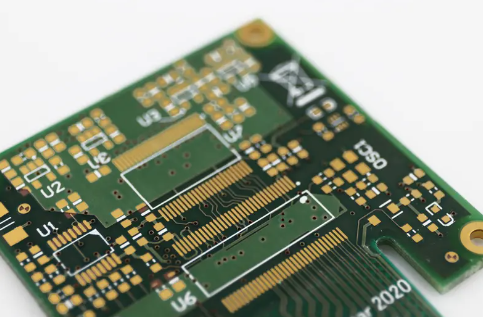
A 16-layer Any Layer HDI PCB IC test board is a high-performance circuit board manufactured using advanced high-density interconnect technology. It is mainly used for chip validation, functional testing, high-speed data analysis, and semiconductor research applications. These PCBs combine laser microvias, Any Layer interconnection structures, and sequential lamination processes to achieve complex high-speed routing and high-density component layouts.
Compared with standard multilayer PCBs, this type of product offers major advantages in high-speed signal integrity, interlayer connectivity, and support for high-density chip packaging.
Main performance features include:
- Supports complex 16-layer structures for advanced high-speed systems.
- Any Layer interconnection technology improves routing flexibility.
- Ultra-fine trace processing supports high pin-count chips.
- High-frequency low-loss materials improve transmission stability.
- Multi-layer power and ground structures optimize signal integrity.
- High-reliability structures support long-term continuous testing environments.
In AI chip and high-speed communication chip testing systems, high-layer-count HDI PCBs have become an essential foundation.
Key Specifications of 16-Layer Any Layer HDI PCBs
Different application scenarios require different IC test board specifications, and PCB parameters directly affect final testing performance.
| Item | Typical Specification Range | Main Purpose |
| PCB Layer Count | 16 Layers | Supports complex high-speed system routing |
| Minimum Trace Width/Spacing | 2.5mil–3mil | Improves routing density |
| Microvia Diameter | 0.1mm–0.15mm | Enables high-density interlayer connections |
| Surface Finish | ENIG / OSP | Improves soldering reliability |
| High-Frequency Materials | Low-loss high-speed materials | Reduces signal attenuation |
| Impedance Control | Within ±5% | Maintains stable high-speed signals |
| Copper Thickness | 1oz–2oz | Enhances power delivery and thermal performance |
These specifications are typically optimized according to chip type, testing frequency, and high-speed interface requirements.
Key Manufacturing Considerations for 16-Layer Any Layer HDI PCBs
Advanced IC test boards require extremely high manufacturing precision, making strict engineering control and quality management essential throughout production.
During the initial PCB design stage, high-speed differential signals, power integrity, and thermal structures must be comprehensively planned.
- Stack-up structure optimization improves high-speed signal isolation.
- High-frequency material matching reduces signal loss.
- Laser microvia processing enables dense interlayer interconnections.
- Any Layer connection design enhances complex routing capability.
- Impedance control analysis improves high-speed signal consistency.
- Via filling and plating strengthen interlayer connection reliability.
- AOI inspection detects ultra-fine circuit defects.
- X-ray inspection checks internal lamination and microvia quality.
- Electrical testing verifies stable high-speed operation.
Complex IC test boards often require signal simulation and thermal analysis technologies to support long-duration high-speed operation.
Why Choose Our 16-Layer Any Layer HDI PCB Products?
High-end chip testing systems demand exceptional PCB precision and stability, making PCB quality directly related to testing results and system reliability.
Our 16-layer Any Layer HDI PCB products offer the following advantages:
- Supports high-layer-count and multi-stage HDI manufacturing.
- Ultra-fine trace capability meets advanced chip packaging requirements.
- High-speed impedance control improves signal integrity.
- Precision laser drilling enhances interlayer connection stability.
- Supports fast prototyping and mass production.
- Comprehensive inspection processes improve product consistency.
- Extensive experience in high-speed test board manufacturing.
- Stable delivery capability for long-term projects.
For AI chips, high-speed CPUs, and 5G chip testing applications, we provide highly reliable HDI PCB product support.
Main Application Areas of 16-Layer Any Layer HDI PCBs
As semiconductor technology continues advancing, high-layer-count HDI test boards are being widely used across multiple advanced industries.
- AI and GPU Chip Testing:High-performance GPUs and AI chips require large amounts of high-speed signal connections, and high-layer-count HDI PCBs improve transmission stability.
- High-Speed CPU Validation Platforms:Complex CPU testing systems often require more PCB layers and stricter impedance control.
- 5G and High-Speed Communication Chips:High-speed communication systems require lower signal loss and superior signal integrity.
- Semiconductor Research Equipment:Advanced research platforms require stable PCB structures for long-term testing operations.
- Data Center and Server Testing:Server chip testing environments typically involve high-frequency, high-speed, and long-duration operation conditions.
Higher Layer Counts, Faster Speeds, and Greater Precision
With the continuous advancement of advanced packaging, AI computing power, and high-speed communication technology, IC test board PCBs are evolving toward higher layer counts, higher density, and lower signal loss. Future PCB manufacturing will focus more on ultra-fine trace processing, stricter impedance control, and more advanced thermal structures, while integrating intelligent manufacturing and automated inspection systems to improve product consistency and production efficiency.
High-frequency low-loss materials, AI-assisted PCB design, and more precise laser processing technologies will further expand the application of 16-layer Any Layer HDI PCBs in advanced chip testing fields.
In modern high-performance chip testing systems, 16-layer Any Layer HDI PCBs are no longer just ordinary circuit boards. They have become critical foundations that directly affect testing accuracy, signal stability, and system reliability. These PCBs meet the demanding requirements of high-speed, high-frequency, and highly integrated chips in complex testing environments while improving overall testing efficiency and long-term operational stability. For companies pursuing high-performance chip testing platforms, choosing high-quality 16-layer Any Layer HDI PCB products will become an important step toward technological advancement and stronger market competitiveness.


")

