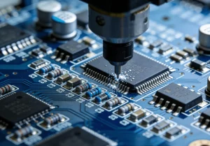
When customers shop for 5G or high-speed communication PCBs, “low-loss material” is often the first phrase they mention. But low-loss does not automatically mean “best.” The right choice depends on frequency, channel length, connector transitions, and your cost target. Many successful products use hybrid stackups—combining standard laminates with low-loss layers only where performance matters.
This guide explains how to choose materials practically—so you can meet performance goals without overpaying.
1) When Do You Actually Need Low-Loss?
Low-loss materials become valuable when your product faces one or more of these conditions:
- Long high-speed channels (backplanes, large line cards)
- Higher frequency RF sections (5G RF paths, antenna feeds, front-end modules)
- Tight margin in eye diagram/jitter budget
- Dense connector transitions and via fields
If your critical links are short and margins are wide, standard high-Tg materials may be enough. If the links are long and fast, material loss becomes a major part of your total channel loss.
2) The Smart Approach: Hybrid Stackups
A hybrid stackup is often the best balance:
- Use standard materials for power/control layers and non-critical nets
- Use low-loss laminates for layers that carry critical differential pairs or RF traces
- Keep a consistent reference plane strategy to preserve return paths
This approach can significantly reduce BOM cost while still delivering the performance you need.
3) Define “Critical Nets” Before You Choose Materials
Material selection should follow design intent. Identify:
- Which lanes are performance-critical
- Which layers those lanes should route on
- Where transitions occur (connectors, via changes, layer swaps)
Once the critical nets are clear, the manufacturer can recommend which layers should use low-loss laminates and which can remain standard.
4) Manufacturing Matters as Much as the Material Name
Even the best laminate won’t save a design if the stackup and geometry are not manufacturable. For consistent results, pay attention to:
- Dielectric thickness windows that are stable in production
- Trace widths/spacings that do not sit at the edge of capability
- Copper roughness and process consistency for repeat builds (manufacturer-dependent)
Ask your supplier to propose a stackup that achieves your impedance targets with comfortable routing geometry—not a “paper-perfect” calculation that is hard to fabricate consistently.
5) Questions to Ask Before You Approve a Material Plan
- Can we achieve the target impedance with realistic trace geometry?
- Do we need backdrill or via optimization to reduce discontinuities?
- Should we concentrate low-loss materials only on critical layers?
- What is the expected production repeatability for thickness and impedance?
6) What to Send for a Fast Material Recommendation
To get an accurate recommendation quickly, provide:
- Frequency band or data rate target
- Board size and layer count
- Target thickness and copper weights
- Critical nets list and approximate routing layers
- Any cost limit or preferred material family
CTA: Send your targets and design constraints. We’ll recommend a practical material + hybrid stackup strategy to balance SI performance and cost.