PCB design is a core part of electronic product development, determining the connection methods between electronic components and the stability of circuit operation. Whether it’s mobile phones, computers, or industrial control equipment, all rely on PCBs as their basic carrier. With the continuous development of electronic technology, PCB design has gradually evolved towards higher density, higher speed, and multi-layered structures.
Basic Concepts of PCB Design
A PCB, or Printed Circuit Board, is a basic structure used to carry electronic components and achieve electrical connections. PCB design refers to the process of using specialized design software to transform circuit schematics into a practically manufacturable circuit board layout and circuit routing. This process requires converting electrical logic into physical structure, enabling stable signal transmission on the circuit board while meeting manufacturing process requirements.
Main Structural Components of a PCB
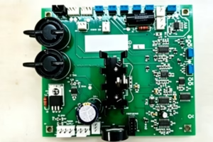
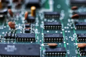
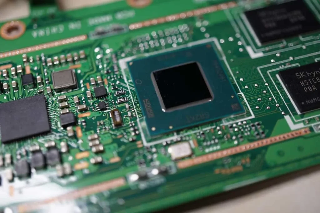
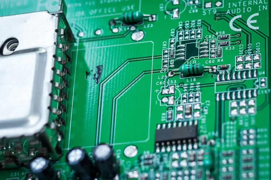
A PCB typically consists of multiple functional layers, each with a specific function. Common structures include a substrate, copper foil layer, solder mask layer, and silkscreen layer. The substrate provides mechanical support and insulation, the copper foil layer handles electrical connections, the solder mask layer protects the circuitry and reduces the risk of short circuits, and the silkscreen layer identifies component locations and parameter information. These structures together constitute a complete circuit carrying system.
Basic PCB Design Process
PCB design is typically completed step-by-step, progressing from circuit logic to physical implementation.
- Schematic Design Stage: Complete the circuit logic connections, determine the relationships between components and signals, and provide a foundation for subsequent design.
- Component Package Matching Stage: Match the components in the schematic to their corresponding packages, ensuring that the physical dimensions are consistent with the actual components.
- PCB Layout Stage: Place components according to the circuit function, optimizing space and signal paths.
- PCB Routing Stage: Complete electrical connections, ensuring signal integrity and power stability.
- Design Rule Check Stage: Detect spacing, short circuits, and connectivity issues to reduce production risks.
These steps are interconnected, and each step affects the final PCB quality.
Key Rules in PCB Design
During the PCB design process, certain electrical and structural rules must be followed to ensure stable circuit operation. Signal lines should be kept as short and straight as possible to reduce interference; power lines need sufficient width to reduce resistance and heat generation; ground lines should maintain a complete return path to avoid signal distortion. Different types of signals need to be rationally zoned, with high-speed and low-speed signals laid out separately to reduce mutual interference.
Common Application Areas and Development Trends
PCB design is widely used in many industries, including consumer electronics, communication equipment, automotive electronics, and medical devices. From smartphones to industrial control systems, circuit functions rely on PCBs. With technological advancements, PCBs are evolving towards higher density, higher frequency, and more complex multi-layer structures, placing higher demands on design capabilities and manufacturing processes.
PCB design is a fundamental technology in electronic engineering. Through rational layout and standardized routing, stable and reliable circuit functions can be achieved. Understanding PCB structure and design processes helps to gain a deeper understanding of the working principles of electronic products and lays a solid foundation for subsequent learning and practice.