


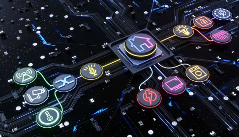
With the rapid development of smart homes, industrial automation, smart healthcare, and smart city technologies, the number of IoT devices continues to grow rapidly. Compared with traditional electronic products, IoT devices must not only achieve stable data transmission but also balance low power consumption, miniaturization, and long-term operational reliability. As the core foundation of IoT hardware systems, PCB (Printed Circuit Board) design directly affects device performance, communication stability, and product lifespan. Therefore, developing high-reliability, highly integrated, and efficient IoT PCB design solutions has become a major focus in modern electronics development.
Core Requirements for IoT Device PCB Design
IoT devices operate in complex environments, so PCB designs must simultaneously meet communication, power efficiency, and reliability requirements.
Miniaturization and High-Integration Design
As IoT terminals become smaller and lighter, PCB space utilization becomes increasingly important.
- HDI (High-Density Interconnect) technology allows more functions to be integrated into limited board space, improving overall device performance
- Microvias and fine-line routing help reduce PCB size while increasing routing efficiency
- Highly integrated layouts combining wireless modules, sensors, and processors reduce overall volume and connection losses
- Compact PCB designs improve portability while also reducing power consumption and material costs
Low-Power Design Optimization
Most IoT devices rely on battery power, making energy efficiency a critical design factor.
- Optimized power routing reduces energy loss and improves battery life
- Low-power MCUs and sleep-mode designs significantly extend operational time
- Proper power and signal routing minimizes additional energy consumption caused by parasitic capacitance
- Dynamic power control for wireless modules reduces unnecessary current usage and improves overall energy efficiency
Wireless Communication and RF Performance
Stable wireless communication is one of the most important functions of IoT devices, making RF design extremely important.
- Different communication protocols such as Wi-Fi, Bluetooth, LoRa, and NB-IoT require different PCB layout strategies
- Antenna areas should be isolated from noisy components to reduce electromagnetic interference
- Proper impedance control and RF trace optimization reduce signal reflection problems
- Effective grounding design improves communication stability and transmission efficiency
Common PCB Structures and Material Solutions for IoT Devices
Different application scenarios require different PCB structures and materials, making proper selection essential.
PCB Solution Comparison Table
| PCB Type | Core Features | Typical Applications |
| HDI Multilayer PCB | High density, compact size | Smart home devices |
| High-Frequency Low-Loss PCB | Strong RF performance | Wireless communication terminals |
| Flexible PCB (FPC) | Bendable and lightweight | Wearable devices |
| Rigid-Flex PCB | High integration capability | Advanced smart terminals |
HDI Multilayer PCB Solution
HDI PCBs have become the mainstream choice for many IoT products.
- Provide higher routing density for complex functional integration
- Microvia structures improve high-speed signal transmission performance
- Multilayer structures isolate power and signal layers to reduce interference
- Commonly used in smart gateways, industrial controllers, and smart home systems
High-Frequency Low-Loss Material Solution
High-frequency materials are becoming increasingly important in wireless communication devices.
- Low dielectric constant materials improve signal propagation speed
- Low-loss materials reduce signal attenuation and improve communication stability
- High-frequency PCBs are especially suitable for 5G IoT terminals and edge computing devices
- Maintain stronger signal integrity in complex RF environments
Flexible and Rigid-Flex PCB Solutions
Wearable and ultra-compact devices require flexible structural designs.
- Flexible PCBs support curved and irregular device structures while improving space utilization
- Rigid-flex boards reduce connector usage and improve overall reliability
- Lightweight designs improve portability and user experience
- Widely used in smart watches, medical monitoring equipment, and portable devices
IoT PCB Manufacturing and Mass Production Optimization
Beyond PCB design itself, manufacturing capability also determines whether IoT products can be produced efficiently and reliably.
Design for Manufacturability (DFM)
Mass production requires balancing cost efficiency and manufacturing stability.
- Standardized component sizes reduce production difficulty and procurement costs
- Reducing complex vias and special structures improves manufacturing yield
- Early DFM analysis minimizes redesign and production issues later in development
- Proper component placement improves SMT assembly efficiency
Automated Manufacturing and Inspection
Automation has become a major trend in IoT PCB production.
- SMT assembly technology improves manufacturing speed and precision
- AOI (Automated Optical Inspection) quickly identifies soldering defects
- ICT (In-Circuit Testing) improves PCB reliability before shipment
- Automated production reduces labor costs while improving product consistency
Long-Term Reliability Verification
IoT devices often need to operate continuously for extended periods, making reliability testing essential.
- Thermal cycling tests verify PCB resistance to environmental stress
- Vibration and drop testing improve durability against physical impact
- RF performance testing ensures stable wireless communication
- Long-term aging tests help identify potential failures before deployment
Future Trends in IoT PCB Development
As smart connectivity continues to expand, IoT PCB technology is also evolving rapidly.
High-Frequency and High-Speed Development
Future IoT systems will increasingly rely on high-speed communication technologies.
- 5G and Wi-Fi 7 will continue driving demand for high-frequency PCBs
- High-frequency low-loss materials will become more important
- Advanced impedance control technologies will see broader adoption
Higher Integration and Miniaturization
IoT devices are becoming smaller, requiring increasingly compact PCB solutions.
- Higher-layer HDI structures will become mainstream
- SiP packaging and embedded component technologies will be adopted more widely
- Smaller and more integrated designs improve product competitiveness
Smart Manufacturing and Green Production
Future PCB manufacturing will focus more heavily on environmental sustainability and intelligent production systems.
- Halogen-free eco-friendly materials are becoming more common
- AI-assisted PCB design is improving development efficiency
- Automation and intelligent inspection technologies will further reduce production costs
As IoT devices continue to expand across industries, PCB design has evolved far beyond simple electrical connectivity and has become a key factor affecting product performance and market competitiveness. From compact layouts and low-power optimization to RF design and mass production efficiency, every design detail directly impacts device stability and user experience. Only by selecting the right PCB structures, materials, and manufacturing strategies for specific applications can manufacturers create high-reliability, high-performance IoT solutions and achieve stronger competitiveness in the future era of intelligent connectivity.