


As the core hub of network communication, the router’s communication backplane PCB board is crucial for signal transmission, power distribution, and module interconnection, directly determining the router’s performance and service life. We have developed a high-adaptability solution to address key pain points such as high-speed transmission and high-density integration, balancing practicality, economy, and scalability.
Core Design Principles
The three core principles support each other to ensure the solution’s feasibility and performance, with details as follows:
- Signal Integrity Priority: Strictly control impedance matching, signal delay, and crosstalk to avoid attenuation and distortion, adapting to the router’s multi-port and high-bandwidth needs.
- Scenario-Adapted Reliability: Optimize heat dissipation, EMI resistance, and corrosion resistance—focusing on miniaturization for home use, high stability for enterprises, and extreme environment resistance for industrial use.
- Economy & Scalability: Select cost-effective materials and processes, while reserving expansion space for future function upgrades.
- These principles lay a solid foundation for the router’s stable operation.
Core Parameters and Material Selection
Core parameters and materials directly affect PCB performance, with targeted selection based on router needs.
Core Parameter Selection
Key parameters are set according to router scenarios and rates, with details as follows:
- Layer Design: 4-layer for entry-level home routers, 6-8 layers for high-end/home enterprise routers, and 10+ layers for high-end industrial routers.
- Line Width & Spacing: 0.8-1.2mm for high-speed signals (line spacing ≥1mm); ≥2mm for core power lines; 50Ω single-ended/100Ω differential impedance for differential signals.
- Hole Diameter: 0.3-0.5mm through holes, <0.2mm microvias for high-density areas, with ±0.05mm tolerance.
- Copper Thickness: 1oz for conventional areas, 2oz for power/high-frequency areas, and 3oz+ for industrial scenarios.
Scientific parameter selection ensures the PCB’s efficiency and durability.
Material Selection Comparison
| Material Type | Core Characteristics | Applicable Scenarios | Advantages | Disadvantages |
| FR-4 Epoxy Substrate | Stable dielectric constant, good heat resistance, cost-effective | Entry/mid-range home routers | Low cost, easy processing, sufficient supply | Large high-frequency loss |
| Rogers RO4350 | Low dielectric constant, low high-frequency loss | High-end home/enterprise routers | Excellent high-speed performance, strong anti-interference | Higher cost, difficult processing |
| Polyimide (PI) | High temperature/corrosion/vibration resistance | Industrial/harsh environment routers | Strong adaptability, high durability | High cost, complex mass production |
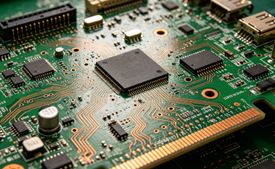
PCB Layout and Wiring Design
Layout and wiring are key to signal quality and heat dissipation, following the principle of partitioned layout and layered wiring.
Partitioned Layout Design
Partitioned layout balances functionality and anti-interference, with specific requirements as follows:
- Clear Functional Zones: Divide into signal transmission, power supply, interface, and heat dissipation areas to avoid interference.
- Nearby Module Arrangement: Place interconnected components close to shorten signal distance; separate heat-generating and sensitive components (≥5mm spacing).
- Expansion Space: Reserve 2-3 expansion interfaces to reduce upgrade costs.
A reasonable layout reduces interference and improves assembly/maintenance efficiency.