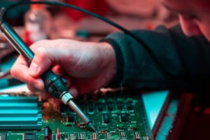
PCB design is an indispensable part of electronic product development, directly affecting circuit stability, anti-interference capabilities, and overall performance. For those new to PCB design, mastering the basic structure, design process, and key rules can help build a comprehensive understanding more quickly, reduce errors in actual projects, and improve design quality.
PCB Basic Structure and Core Components
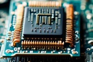
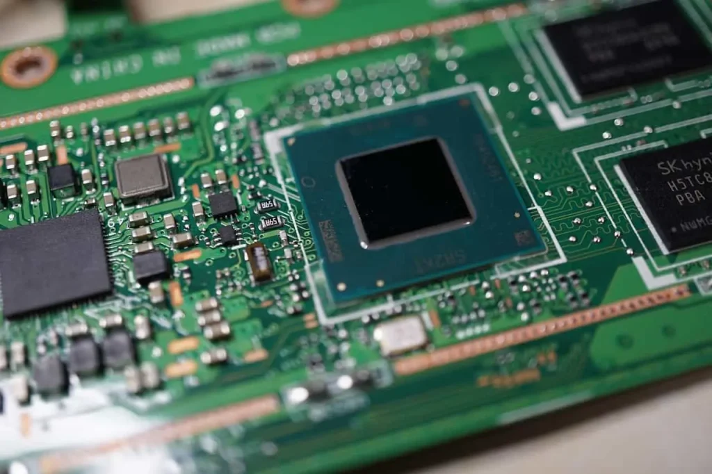
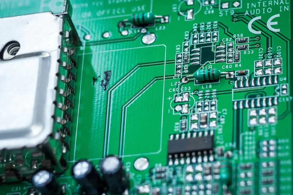
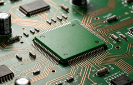
A PCB (Printed Circuit Board) mainly consists of a substrate, copper foil traces, solder mask, and silkscreen layer. The substrate typically uses FR-4 material, which has good insulation properties and mechanical strength. The copper foil layer is responsible for carrying electrical connections and is the core path for signal transmission. The solder mask layer covers the copper foil surface to prevent oxidation, reduce the risk of short circuits, and improve soldering accuracy. The silkscreen layer is used to identify component numbers, polarity, and functional information, facilitating subsequent assembly and maintenance.
Schematic Design and Logic Representation
Schematic design is a crucial early step in PCB design, used to express the logical relationships of the circuit. At this stage, appropriate components need to be selected based on functional requirements, and the electrical connections need to be drawn. The clarity of the schematic diagram directly affects the efficiency of subsequent PCB layout. A chaotic structure can easily lead to incorrect connections or repetitive design. Maintaining consistent signal naming conventions helps improve the readability of the overall design.
Key Points of PCB Layout Design
Layout design determines the spatial distribution of components on the circuit board, which has a significant impact on performance. A reasonable layout can reduce signal interference, improve heat dissipation efficiency, and optimize routing difficulty. During design, it is necessary to plan the layout in conjunction with the circuit function, separating analog and digital circuits as much as possible to avoid mutual interference. At the same time, the height of components, mounting direction, and maintenance space should also be considered to make the overall structure more reasonable.
Routing Rules and Signal Integrity Control
Roading is one of the most critical steps in PCB design and must follow certain electrical and structural rules. High-speed signals should maintain short paths and straight lines as much as possible, reducing unnecessary bends and vias. Power lines need to be appropriately widened to reduce impedance and improve power supply stability. Ground lines should form a complete return path to avoid signal interference caused by breaks.
In the actual routing process, the following points should be emphasized:
- Differential signal control: Maintain equal length and spacing in the routing to reduce signal deviation.
- Via Usage Control: Avoid excessive vias that could affect signal integrity and impedance consistency.
- High-Speed and Low-Speed Signal Separation: Reduce interference from high-speed signals to low-speed signals.
- Power Supply and Signal Isolation: Prevent power supply noise from affecting sensitive signal lines.
- Return Path Optimization: Ensure ground plane integrity and improve anti-interference capability.
Appropriate application of these rules can significantly improve the stability and reliability of the PCB.
Common Design Tools and Practical Techniques
PCB design typically relies on EDA software, such as Altium Designer, KiCad, and PADS. During the design process, rule checking functions can be used to identify insufficient spacing, short circuits, or disconnections in advance, improving design accuracy. Appropriate use of automatic routing functions can improve efficiency, but critical lines still require manual optimization to ensure signal quality. Maintaining a clear design hierarchy and consistent naming conventions facilitates later maintenance and modifications.
PCB design involves multiple stages, including structural understanding, logical expression, layout planning, and routing control. By systematically learning the basics and continuously practicing, one can gradually improve design capabilities, make circuit performance more stable, and lay a solid foundation for the development of complex electronic products.