


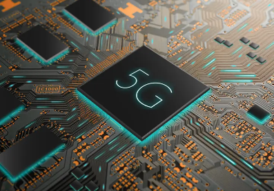
As 5G communication moves into large-scale deployment, data transmission rates and operating frequency bands continue to increase. Printed circuit boards (PCBs) are no longer just interconnection carriers; they have become a critical factor determining signal quality and system performance. In scenarios such as millimeter-wave communication, base stations, and high-speed data centers, PCB material properties—such as high-frequency loss, dielectric stability, and structural consistency—directly affect signal integrity and system reliability. Therefore, high-frequency and high-speed material solutions have become a key focus in 5G PCB design.
Core Material Requirements for 5G High-Frequency PCBs
In high-frequency 5G environments, signals are more sensitive to loss and require strict material performance control to ensure stable transmission.
Low Dielectric Constant (Dk) Stability
Dielectric constant stability directly affects signal propagation speed and phase consistency.
- Maintain minimal Dk variation across frequencies
- Prevent signal delay and phase distortion
- Ensure consistent performance in multilayer structures
Low Dielectric Loss (Df) Control
Dielectric loss determines energy attenuation in high-frequency transmission.
- Lower Df reduces signal loss
- Improves long-distance communication capability
- Enhances transmission efficiency at high frequencies
Thermal and Dimensional Stability
High-power operation requires materials with strong stability under thermal stress.
- Stable dielectric properties at high temperatures
- No deformation under long-term operation
- Reliable multilayer lamination stability
Mainstream 5G High-Frequency PCB Material Types
Different applications require different material systems to balance performance and cost.
PTFE (Polytetrafluoroethylene) Material System
PTFE is one of the most mature high-frequency PCB materials.
- Extremely low dielectric loss
- Suitable for millimeter-wave and radar systems
- Excellent high-frequency stability
- High processing difficulty and cost
LCP (Liquid Crystal Polymer) Material System
LCP is widely used in advanced 5G flexible and miniaturized designs.
- Extremely low moisture absorption
- Excellent flexibility for antenna applications
- Strong high-frequency performance
- Suitable for compact communication modules
Modified Epoxy Resin System
A cost-effective solution for medium and high-frequency applications.
- Low cost and mature processing
- Stable manufacturing yield
- Suitable for below 30GHz applications
- Widely used in communication modules
High-Frequency Composite Materials
Composite systems balance performance and cost flexibility.
- Balanced dielectric and mechanical properties
- Widely used in base stations
- Customizable dielectric performance
- Suitable for multilayer complex structures
Key PCB Structural Design Optimization Points
Even with excellent materials, improper design can still degrade signal performance.
Impedance Matching Design
Proper impedance control ensures signal integrity.
- Precise control of trace width and dielectric thickness
- Maintain consistent impedance across signal paths
- Reduce reflection and signal distortion
- Improve high-speed transmission stability
Multilayer Stack-Up Optimization
Layer configuration plays a key role in reducing interference.
- Proper arrangement of signal and ground layers
- Minimize electromagnetic interference
- Improve shielding performance
- Optimize return current paths
Via and Routing Optimization
Via structures significantly affect high-frequency performance.
- Reduce via count and length
- Use back-drilling to reduce parasitic effects
- Optimize high-speed routing paths
- Minimize signal reflection and loss
Material Performance Comparison and Selection Reference
Different materials vary significantly in performance, cost, and frequency suitability.
| Material Type | Dielectric Loss (Df) | Processing Difficulty | Cost Level | Frequency Range |
| PTFE | Extremely Low | High | High | >60GHz |
| LCP | Low | Medium | Medium-High | 30–60GHz |
| Modified Epoxy | Medium | Low | Low | <30GHz |
Material Selection Logic
Selection depends on application requirements and trade-offs.
- High-frequency systems prioritize low-loss materials
- Cost-sensitive designs use epoxy-based systems
- Miniaturized devices prefer LCP solutions
- Ultra-high-frequency applications rely on PTFE
Development Trends of 5G High-Frequency PCB Technology
As communication technologies advance toward higher frequency bands, PCB materials and processes continue to evolve.
Continuous Development of Ultra-Low Loss Materials
Material innovation focuses on reducing dielectric loss further.
- Support higher frequency transmission
- Reduce energy loss in millimeter-wave bands
- Enabl future 6G communication systems
Multi-Material Hybrid Structures
Combining materials optimizes overall performance.
- Different layers use different materials
- Balance performance and cost
- Increase design flexibility
High-Precision Manufacturing Improvements
Manufacturing accuracy directly affects high-frequency performance.
- Improve circuit fabrication precision
- Reduce multilayer alignment deviation
- Enhance mass production consistency
In 5G high-frequency applications, PCB material selection and structural design form a highly integrated engineering system. As communication systems continue evolving toward higher frequencies, advanced PCB materials and precision design technologies will remain essential foundations for achieving faster, more stable, and lower-loss communication performance.