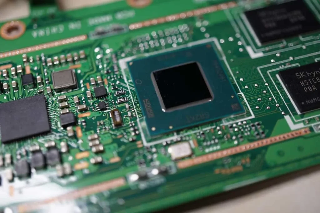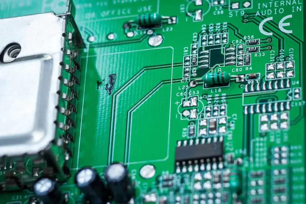

High frequency PCB material selection is not only about choosing a low-loss laminate. The material must also match the signal type, operating frequency, routing length, stack-up, copper profile, thermal conditions, assembly process, and production requirements.
A material that works well in one RF or high-speed design may not be suitable for another. A project can face signal loss, impedance variation, poor repeatability, or unnecessary cost when the material decision is made from a short datasheet comparison alone.
For high-frequency projects, buyers should first define what the circuit needs to achieve. Then the PCB material, copper type, dielectric thickness, and stack-up can be reviewed as one system.
For fabrication support related to RF, microwave, and low-loss laminate requirements, link relevant wording to High Frequency PCB.
Why Material Selection Creates Risk in High Frequency PCB Projects
A PCB laminate affects the dielectric environment around a signal trace. This influences impedance, signal loss, propagation behavior, and routing dimensions.
Material selection becomes more important when a board includes:
- RF signal paths
- Microwave circuits
- High-speed digital interfaces
- Differential pair routing
- Long controlled-impedance traces
- Antenna feed structures
- Communication backplanes
- Low-loss channel requirements
- Mixed RF and digital sections
The risk is not simply choosing the wrong material family. The risk is choosing a material without confirming how it will behave within the finished stack-up.
A high-frequency PCB should be reviewed together with layer order, dielectric thickness, copper weight, copper roughness, trace geometry, and reference-plane structure.
Material Data Must Be Compared Under Matching Conditions
Material data sheets often list dielectric constant and dissipation factor values. These values are useful, but they should not be compared without checking the test conditions.
A Dk value can depend on the test method, test frequency, material construction, resin content, and measurement direction. A Df value can also vary with test conditions and material structure.
Do not compare Dk values without checking the test method
Two materials may show similar Dk values but use different test conditions. Comparing the numbers without checking frequency and method can lead to the wrong design assumption.
For controlled impedance routing, the useful question is not only “What is the Dk value?” It is also “Which Dk value should be used for this stack-up and this routing condition?”
Do not assume one data-sheet value represents every layer construction
Core thickness, prepreg construction, glass style, and resin content may affect the dielectric environment around a trace. A multilayer stack-up should use material data that matches the intended construction as closely as possible.
Ask whether the value supports design or material comparison
Some values are useful for general material comparison. Others are more useful for impedance calculation or field-solver input. These are not always the same purpose.
When stack-up, trace width, dielectric thickness, or impedance requirements are discussed, link relevant wording to Impedance Controlled PCBs.
Loss Risk Is More Than Dissipation Factor
Dissipation factor is often used as a material-selection reference for high-frequency PCB projects. It is important, but it is not the only source of signal loss.
The final loss of a channel can also be affected by copper roughness, trace length, conductor width, dielectric thickness, via transitions, surface finish, and the frequency range of the signal.
Low Df does not remove all channel-loss risk
A lower Df material can help reduce dielectric loss. However, a long signal path, rough copper, poor return path, or repeated layer transitions can still create a loss problem.
A material review should therefore include the complete signal path, not only a laminate datasheet.
Copper roughness may affect higher-frequency signal behavior
At higher frequencies, current distribution near the conductor surface becomes more important. Copper surface profile can therefore affect conductor loss.
The selected copper treatment should be considered with the laminate and the intended signal path. It should not be treated as a separate purchasing detail after the electrical design is finalized.
Surface finish should be reviewed for the application
Surface finish can affect assembly, corrosion protection, solderability, and some RF-related design choices. The correct choice depends on the PCB structure and end-use requirements.
The goal is not to select a surface finish from habit. It is to confirm that the finish is compatible with the electrical, fabrication, and assembly needs of the project.
Stack-Up Risk Can Override a Good Material Choice
A suitable material does not guarantee a suitable high-frequency board. The finished stack-up controls the distance between signal traces and reference planes. It also affects trace width, impedance, coupling, and return-path behavior.
A material should be selected together with the stack-up, not before it.
Dielectric thickness changes impedance calculations
A trace width that works on one dielectric thickness may not work on another. When the signal-to-plane distance changes, the trace geometry often needs to change as well.
This is why routing rules should be reviewed against the actual production stack-up.
Reference planes need to support the intended signal path
Critical RF, high-speed, and controlled-impedance traces need suitable reference structures. A nearby and continuous reference plane helps provide a more predictable return path.
A trace routed across a split plane, void, slot, or interrupted reference area may create signal-integrity risk even if the material selection is appropriate.
Mixed-material structures need early review
Some projects combine different material types within one board structure. These mixed stack-ups may be useful when RF and digital sections have different needs.
However, they also require early review of lamination compatibility, thickness control, layer order, fabrication notes, and assembly conditions.
For projects that need complex layer structures and internal routing, link relevant wording to Multilayer PCB
Thermal and Assembly RImpedance Controlled PCBsequirements Can Change the Material Decision
A high-frequency laminate must also survive the manufacturing and operating conditions of the finished product.
Electrical behavior is only one part of the decision. Thermal exposure, assembly profile, mechanical stress, moisture exposure, and board construction can also matter.
Do not select low-loss material without checking thermal requirements
A material may have suitable electrical properties but may need further review for assembly temperature exposure, repeated thermal cycles, or the mechanical requirements of the finished board.
This is especially important for boards with dense components, BGA packages, large copper areas, or repeated rework exposure.
High Tg and high-frequency needs are not always the same
High Tg material selection is usually related to thermal requirements. High-frequency material selection is usually related to electrical behavior and loss control.
Some projects may need both. Others may need only one. The material choice should match the actual risk rather than combining specifications by default.
When thermal material requirements are relevant, link to High Tg PCB.
Assembly data should be reviewed before material release
For PCBA projects, component package types, soldering profile needs, thermal pads, board thickness, and assembly access can affect the final fabrication plan.
For BOM review, assembly drawings, pick-and-place files, and testing requirements, link relevant wording to PCBA processing.
Common High Frequency PCB Material Selection Mistakes
Selecting material only by the lowest Df value
The lowest Df value does not automatically produce the best board. The signal path, copper profile, layer construction, routing density, and cost target should also be reviewed.
A lower-loss material may not be necessary for every signal layer or every section of the board.
Using generic FR4 wording for a controlled design
“FR4” is a broad material category. It does not define the exact electrical behavior, resin content, glass style, or thermal performance required for a controlled high-frequency design.
Where electrical targets matter, the material family and intended stack-up should be identified more clearly.
Copying a material stack-up from another project
A prior stack-up may use different layer count, board thickness, copper weight, signal routing, component density, or assembly requirements.
A previous material choice should be treated as a starting point, not a final production decision.
Ignoring copper profile during early design review
Copper roughness can affect loss behavior. It should be discussed when the project has longer high-frequency signal paths, stricter channel-loss requirements, or sensitive RF routing.
Finalizing routing before material review
Trace widths and differential-pair spacing should match the reviewed stack-up. If the material or dielectric thickness changes after layout release, impedance and routing assumptions may need to be checked again.
What Buyers Should Confirm Before Quotation
The material review is more accurate when the manufacturer receives a complete technical package.
| Project Information | Why It Matters |
|---|---|
| Operating frequency or signal type | Helps identify electrical material requirements |
| Gerber files | Shows routing, copper features, pads, and board structure |
| Stack-up notes | Defines layer arrangement and dielectric requirements |
| Controlled impedance table | Identifies target values and affected layers |
| Board thickness target | Supports core and prepreg planning |
| Material requirement or approved list | Clarifies customer restrictions |
| Copper weight requirement | Affects signal geometry and thermal planning |
| Surface finish requirement | Supports fabrication and assembly review |
| Quantity and project stage | Helps define production planning needs |
| Assembly data, if applicable | Supports component and thermal review |
For Gerber files, fabrication notes, stack-up revisions, and engineering review, link relevant wording to PCB design.
How to Compare Material Options More Reliably
Material comparison should use the same decision framework for each option.
| Buyer Check | Why It Matters | What to Confirm |
| Dk comparison | Supports impedance planning | Test method, frequency, material construction |
| Df comparison | Supports dielectric-loss review | Matching test conditions and relevant frequency |
| Copper treatment | Can affect conductor loss | Copper profile and foil type |
| Stack-up fit | Affects routing and impedance | Dielectric thickness and reference planes |
| Thermal fit | Supports assembly and product conditions | Process and operating temperature needs |
| Fabrication fit | Affects manufacturing planning | Lamination and layer-construction requirements |
| Supply approval | Supports controlled sourcing | Approved material family or customer restrictions |
The final choice should be confirmed from the actual project files. A material datasheet alone does not replace stack-up review, impedance planning, or fabrication review.
Preparing for Production Review
Before production release, confirm the signal layers, material direction, dielectric thickness, copper assumptions, stack-up, controlled impedance targets, and assembly requirements.
A high-frequency PCB project should not be released based only on a material name or a single Dk or Df value. The relevant properties must match the actual layer construction and signal path.
For RF and low-loss material projects, you may also need a separate Rogers PCB review when the design specifically requires a Rogers laminate family or an approved RF material direction.
For engineering review and quotation support, please send your Gerber files, stack-up notes, impedance requirements, material notes, and BOM for PCBA projects to sales@toplinecircuit.com.