


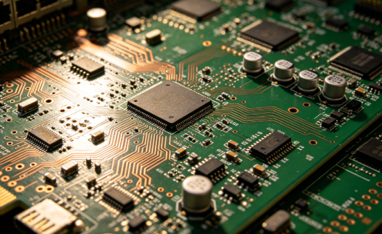
As the core hub of network communication, the performance stability, data transmission rate and reliability of switches directly depend on the design and implementation of the communication backplane PCB board. The communication backplane PCB board is the connection carrier for all internal functional modules of the switch, undertaking key responsibilities such as high-speed signal transmission, power distribution, and module interconnection, and is the “neural network” ensuring the efficient operation of the switch. In response to the high requirements for switch bandwidth, density, and stability in current scenarios such as data centers, industrial control, and telecommunications operators, combined with years of PCB design experience, we have created a multi-scenario, high-performance, and high-reliability switch communication backplane PCB board solution that balances signal integrity, heat dissipation efficiency, and manufacturability to meet the application needs of switches at different levels.
Core Design Premise of the Solution: Scenario Positioning and Performance Indicators
The design of the switch communication backplane PCB board must be guided by scenario requirements, with clear core performance indicators to ensure the implementability and adaptability of the solution. Differences in environmental conditions and bandwidth requirements of different application scenarios directly determine the design parameters of the backplane PCB board. The specific scenario adaptation and core indicators are shown in the following table:
| Application Scenario | Core Scenario Requirements | Backplane PCB Board Adaptation Requirements |
| Data Center | 100G/400G high-speed transmission, multi-module parallelism, high heat dissipation pressure | Ultra-high density interconnection, low-loss materials, enhanced heat dissipation design |
| Industrial Control | -40℃~75℃ extreme temperature, electromagnetic interference resistance, long-term stable operation | Industrial-grade temperature-resistant materials, enhanced EMC design, corrosion-resistant surface treatment |
| Telecommunications Operation | Long-term stability, scalability, low maintenance costs | Modular design, easy maintenance structure, high-reliability testing |
Based on the above scenario differences, the solution defines unified core performance indicators to ensure full-scenario adaptability:
- Signal Transmission Rate: Covering 10G~400G to meet the bandwidth needs of switches at different levels
- Impedance Control Accuracy: Reaching ±5% to ensure the integrity of high-speed signal transmission
- PCB Layers: Can be flexibly designed as 16~40 layers according to requirements to adapt to modules of different complexities
- Operating Temperature: Adapting to -40℃~85℃, compatible with extreme and conventional working environments
Material Selection: Balancing Performance, Cost and Durability
Material selection directly determines the signal transmission quality, heat dissipation efficiency and service life of the backplane PCB board. The solution follows the principle of “performance first, cost adaptation”, and accurately selects suitable materials for different layers and functional requirements. The specific selection details are shown in the following table:
| PCB Board Layer/Function | Selected Materials | Material Characteristics and Advantages |
| Core Signal Layer | High-performance materials such as Nelco 4000-13si | Low dielectric constant (Dk=3.4), low loss tangent (Df=0.008), reducing signal dielectric loss and crosstalk |
| Ordinary Signal Layer/Power Layer | Modified epoxy resin material | Meeting basic electrical performance and effectively controlling solution costs |
| Copper Foil | 1oz~3oz high-purity electrolytic copper (2oz~3oz for power/ground layers) | Improving signal conduction efficiency and heat dissipation performance, reducing power impedance and heat generation |
| Surface Treatment | Electroless Nickel Gold process | Anti-oxidation, anti-corrosion, improving connector soldering reliability and adapting to harsh industrial environments |
High-Speed Signal Integrity Design: Solving Core Transmission Pain Points
With the improvement of switch transmission rate, problems such as signal reflection, attenuation, and crosstalk have become increasingly prominent. The solution comprehensively ensures high-speed signal integrity through refined design. The specific design points are as follows:
- Lamination Design: Adopting a symmetrical structure and following the principle of “signal layer-reference plane layer” alternating arrangement. For backplanes with 16 layers or more, 6~8 reference plane layers are set to ensure that each high-speed signal line has a complete and continuous ground plane or power plane below, shortening the signal return path and reducing interference.
- Impedance Matching: The impedance of Ethernet differential pairs is controlled at 100Ω, and the impedance of single-ended signals is controlled at 50Ω. The line width, line spacing and layer thickness are accurately designed through professional tools to ensure that the impedance deviation does not exceed ±5%.
- Differential Pair Routing: Strictly control the equal length of P and N lines in the differential pair, with an error not exceeding ±5mil to avoid signal distortion; the spacing between different differential pairs follows the “3W” rule, and ground isolation is used when necessary to reduce crosstalk.
- Via and Layer Change Processing: High-speed signal lines should avoid layer changes as much as possible. If layer change is required, add ground vias near the vias and use laser drilling technology to reduce via stub length, avoiding resonance and reflection.
- Clock Signal Protection: Clock signals are routed first, adopting ground shielding treatment. Ground lines are laid in parallel on both sides with dense ground vias, away from high-speed differential pairs and power noise sources to ensure clock stability.
Power Integrity and Heat Dissipation Design: Ensuring Long-Term Stable Operation
The stability of power supply and heat dissipation efficiency are the core supports for the long-term reliable operation of the backplane PCB board. The solution achieves multi-dimensional protection from two aspects: power filtering and heat dissipation optimization.
Power Integrity Design Points
- Multi-layer power/ground plane design to build a low-impedance power loop and effectively reduce power noise.
- Near the power pins of high-heat devices, a combination of multi-capacitance decoupling capacitors is arranged nearby (0.1µF for high-frequency noise filtering, 10µF for energy storage filtering), and low ESR/ESL ceramic capacitors are selected to improve filtering effect.
- A π-type filter circuit is adopted at the power inlet to suppress internal and external noise conduction, and different voltage domains are reasonably divided to avoid power interference.
Heat Dissipation Design Points
- A large-area exposed copper heat dissipation pad is designed at the bottom of high-heat devices, and a dense array of heat dissipation vias is arranged to connect to the internal ground plane or heat dissipation layer for rapid heat conduction.
- The backplane of high-end switches reserves space for heat sink and fan installation, and cooperates with an intelligent temperature control system to dynamically adjust heat dissipation efficiency.
- A circle of ground vias is arranged around the edge of the PCB board to balance electromagnetic compatibility and auxiliary heat dissipation, avoiding local heat accumulation.
- Optimize component layout, disperse high-heat devices, and keep them away from sensitive signal areas to reduce thermal interference.
Manufacturability and Reliability Design: Reducing Costs, Increasing Efficiency and Improving Durability
The solution balances production efficiency and product durability, reducing production costs and later maintenance costs through process optimization and full-process testing. The specific design points are as follows:
- Process Adaptation: Control the size and thickness of the PCB board, adopt a symmetrical lamination design to reduce stress deformation during manufacturing; select standard-sized vias to reduce drilling difficulty and costs.
- Connection Reliability: Adopt press-fit connector technology to improve connection stability and facilitate later module replacement and maintenance.
- Full-Process Testing: Conduct temperature shock testing, vibration testing, salt spray testing, HALT/HASS testing, etc., to ensure stable operation in extreme environments.
- Maintenance Convenience: Reserve test points for key signals, power supplies, and grounds to facilitate later fault diagnosis and debugging and improve maintenance efficiency.
Solution Adaptability: Covering the Needs of the Full Series of Switches
In response to the differentiated needs of switches with different architectures, the solution has flexible adaptability and can be flexibly adjusted according to bandwidth, number of modules, and installation scenarios. The specific adaptation solutions are shown in the following table:
| Switch Architecture Type | Backplane PCB Board Design Adaptation | Core Advantages |
| Traditional Backplane Architecture | Large-size design, optimized single-side card insertion layout | Stable signal transmission, adapting to the needs of mid-to-low-end switches |
| Orthogonal Backplane Architecture | Central orthogonal PCB design to achieve double-sided high-density interconnection | Improving bandwidth capacity and space utilization, adapting to mid-end switches |
| Orthogonal Direct Connection Architecture (High-End) | Eliminating the central backplane, directly connecting service boards and switching fabric boards through high-speed connectors | Eliminating backplane signal loss and space limitations, adapting to high-end core switches |
The design and implementation of the switch communication backplane PCB board is a systematic project integrating multiple technologies and balancing multiple factors. Through accurate scenario positioning, scientific material selection, refined routing design and multi-dimensional optimization strategies, this solution effectively solves the core pain points such as interference, heat dissipation and reliability in high-speed signal transmission, and can meet the application needs of multiple scenarios such as data centers, industrial control and telecommunications operations. The solution not only ensures the efficient and stable operation of the switch, but also has good scalability and maintainability, reducing the total life cycle cost of the equipment, providing a solid hardware support for the upgrading of switch products, and helping the high-quality development of the network communication industry.